3. Щелкните ОК, чтобы закрыть диалоговое окно.
Multisim базируется на промышленном стандарте SPICE 3F5. Ее поддерживаемые модели созданы с использованием стандартного синтаксиса SPICE. Вы можете создать модель, используя Model Makers и назначая значения параметров модели примитива или создавая модель-подсхему (subcircuit model).
6.6.2.1 Создание модели с использованием генераторов моделей
►Чтобы использовать модель, созданную Model Makers:
1.Выберите Model ID в диалоговом окне Select a Model.
2.Щелкните по кнопке Start Model Maker. Появится диалоговое окно Select Model Maker.
3.Выберите Model Maker, который вы хотите использовать для создания модели.
4.Щелкните Accept для продолжения начала процесса создания модели. Щелкните Cancel, чтобы вернуться на закладку Model диалогового окнаComponent Properties.
5.Аналоговые Model Makers описаны в разделе «Создание моделей компонентов с использованием Model Makers», где есть процедуры для отдельных Model Makers. А RF модели описаны в «RF Model Makers».
6.Когда вы введете всю требуемую информацию в диалоговом окне Model Maker, щелкните ОК. Данные модели, что вы только что создали, появятся в поле Model Data.
6.6.2.2 Создание модели примитива
Некоторые устройства имеют SPICE модели примитива. Эти устройства перечислены в таблице ниже. Модель примитива — это модель, которая определяется набором параметров. Они используются как базовые строительные блоки в схемах и подсхемах.
|
National Instruments Corporation |
219 |
Multisim User Guide |
Пример модели примитива для 2n2222a NPN BJT Transistor (NPN биполярный транзистор) следующая. Первая строка модели примитива начинается с утверждения, .MODEL, за которым следует имя модели и тип примитива. В примере ниже модель названа «2N2222A» тип примитива «NPN». Последующие строки модели определяют параметры NPN BJT. Заметьте, что все они начинаются с «+». Детали, относящиеся к параметрам, можно найти в «Multisim Component Reference Guide». Вам не нужно определять все параметры, все, что здесь опущены, добавляются значениями по умолчанию.
.MODEL 2N2222A NPN
+IS=2.04566e-13 BF=296.463 NF=1.09697 VAF=10 +IKF=0.0772534 ISE=1.45081e-13 NE=1.39296 BR=0.481975 +NR=1.16782 VAR=100 IKR=0.100004 ISC=1.00231e-13 +NC=1.98587 RB=3.99688 IRB=0.2 RBM=3.99688 +RE=0.0857267 RC=0.428633 XTB=0.1 XTI=1
+EG=1.05 CJE=1.09913e-11 VJE=0.99 MJE=0.23 +TF=2.96787e-10 XTF=9.22776 VTF=25.2257 ITF=0.0793144 +CJC=3.1941e-11 VJC=0.4 MJC=0.85 XCJC=0.901093 +FC=0.1 CJS=0 VJS=0.75 MJS=0.5
+TR=3.83883e-07 PTF=0 KF=0 AF=1
За дальнейшей информацией, относящейся к моделям примитивов, пожалуйста обратитесь к «Multisim Component Reference Guide» или к «SPICE 3F5 user manual» (http://bwrc.eecs.berkeley.edu/Classes/IcBook/SPICE/).
6.6.2.3 Создание модели-подсхемы (Subcircuit Model)
Многие электронные устройства не представлены примитивами, но они еще хорошо походят как SPICE модели. Subcircuit Models используются для ввода характеристик этих моделей. Подсхемы моделей создаются из набора устройств, которые содержат модели примитивов,
|
National Instruments Corporation |
220 |
Multisim User Guide |
![]()
источников напряжения и/или тока, и/или других моделей-подсхем.
Вы можете либо создать модель-подсхему из набросков, впечатывая их в окно данных модели, или можете вначале начертить схему в Multisim и экспортировать ее в SPICE netlist, а затем уже модифицировать для использования в модели-подсхеме.
Все модели-подсхемы должны начинаться со строки, которая начинается с утверждения
.SUBCKT, за которым следует имя модели-подсхемы и внешние узлы подсхемы, которые будут соединяться с другими компонентами. Подсхема должна заканчиваться утверждением .ENDS.
.SUBCKT <SubcircuitName> <N1> <N2> <N3> <N4>
…
.ENDS SubcircuitName
Модель-подсхема определяется по имени и соединяется внутренними устройствами, которые и создают подсхему. Например, для определения, что резистор 100kΩ со ссылочным указателем (reference designator) R1 соединен с узлами 4 и 5, вы должны написать:
R1 4 5 100k
Пример модели-подсхемы следующий:
Это подсхема для следующей схемы, начерченной в Multisim:
|
National Instruments Corporation |
221 |
Multisim User Guide |
LTSpice. Как создать spice модель из графической ВАХ?
Присоединяйтесь к обсуждению
Вы можете написать сейчас и зарегистрироваться позже.
Если у вас есть аккаунт, авторизуйтесь, чтобы опубликовать от имени своего аккаунта.
Содержание
- Introduction
- Simulation, what is it and why is it necessary?
- What can we simulate using SPICE?
- What are SPICE Models?
- Signal Sources
- Placing and Configuring a Source
- Using a CSV file as a Source
- Configuring and Running a Simulation
- Defining Variants
- The Schematics to Simulate
- Circuit and Model Verification
- Preparing to Simulate
- Including Measurement Probes
- Analysis Setup & Run
- Operating Point Analysis
- DC Sweep
- Transient
- AC Sweep
- Additional Analyses
- Advanced Spice Options
- Running all of the Analyses
- Performing Simulation Measurements
- Working with the Measurement Results
- Sensitivity Analysis
- Schematic Design for Simulation
- Conditions Required for Simulation
- Resolving Model Errors
- Adding Models to the Schematic Components
- Working with File-based Libraries and Models
- Placing a Simulation-ready Component
- Placing a Component when you only have the Model
- Placing a Simulation-Ready Component from the Manufacturer Part Search Panel
- Adding a Model to a Placed Component
- Choose the Source of the Model
- Browse and Select the Model
- Mapping the Model Pins to the Component Symbol Pins
- Creating a new Model File
- Attaching a Model in the Library Editor
- Working with Workspace Components and Models
- Editing the Workspace Component
- Adding a Simulation Model to the Component
- Saving the Updated Workspace Component
- Simulation, finding the Balance between Accuracy and Performance
- Results Display and Analysis
- Working with Plots
- Measurement Cursors
- Defining a Mathematical Expression
- Adding a New Plot
- Working with Digital Plots
- Working with Plots
- What is a SPICE netlist and how to read it?
- Simulation Troubleshooting
- Trouble-shooting simulation analysis failures
- General simulation convergence troubleshooting
- Convergence troubleshooting steps
- DC Sweep Analysis troubleshooting
- Transient Analysis troubleshooting
Полное содержание
Introduction
A circuit is a set of components connected together to deliver the functionality and performance that your product requires. The parameters of the components you need in the circuit can be determined by:
- Manual mathematical calculations.
- Сreating a prototype of the actual design, and then testing it.
- Computer-based mathematical simulation, aka SPICE.
The most efficient and cost-effective option is the use of modern methods of mathematical simulation, using Computer-Aided Design (CAD) systems.
Modern electrical circuit CAD systems combine the ability to simulate circuits that include both analog and digital devices. The use of computer simulation makes it possible to experiment, obtain real circuit characteristics, evaluate possible risks in the device, and also achieve the implementation that best delivers the product’s intended operational range and characteristics.
This guide covers the basic principles of SPICE simulation, how to avoid mistakes, and lots of information on learning how to use the tool.
Simulation, what is it and why is it necessary?
The main purpose of simulating the function of an electronic device is to represent and analyze the performance of the design. The jump from experimental methods to computer software simulation happened quite a long time ago. However, it is impossible to imagine the design of even the simplest device without the capabilities that simulation offers.
Using a simulation program makes it possible to analyze all modes of the device being designed without possible damage, to determine parameters and characteristics that are difficult to measure in real conditions, and to perform measurements that might otherwise require the use of expensive measurement equipment. And the results of these simulations can conveniently be grouped on one plot, they can use several axes, you can change the display color, take measurements directly from the plots, share the results with colleagues, and much more.
SPICE (Simulation Program with Integrated Circuit Emphasis) was developed as an open-source software package, which has led to its broad popularity and continued development. Altium’s Mixed Simulation (MixedSim) technology uses an improved core based on SPICE algorithms and is designed to simulate analog, digital or mixed analog-to-digital device electrical circuits.
This guide will cover not only the mechanisms for obtaining basic circuit characteristics, but also the features of circuit design for simulation, the process of adding models to circuit elements, and the description of the Netlist document and its application.
What can we simulate using SPICE?
Altium’s simulation technology is under active development, including the variety of supported models and model types (including Pspice & LTSpice), the underlying algorithms, and the available types of circuit analyses.
The simulator supports the following types of analyses:
- Operating Point — determines the dc operating point of a circuit, with inductors shorted and capacitors opened.
- Poles and Zeros of transfer function — used to determine the stability of a single input, single output linear system, by calculating the poles and/or zeros in the small-signal ac transfer function for the circuit. The dc operating point of the circuit is found and then linearized, small-signal models for all non-linear devices in the circuit are determined. This circuit is then used to find the poles and zeros that satisfy the nominated transfer function.
- DC Transfer function — (DC small signal analysis) calculates the DC input resistance, DC output resistance and DC gain, at each voltage node in the circuit.
- DC sweep — generates output like that of a curve tracer. Used to sweep variables, including temperature, voltages and currents from sources, resistances and conductivity.
- Transient analysis — generates output similar to that normally shown on an oscilloscope, computing the transient output variables (voltage or current) as a function of time, over the user-specified time interval. An Operating Point analysis is automatically performed before a Transient analysis to determine the DC bias of the circuit unless the Use Initial Conditions parameter is enabled.
- Fourier analysis — Fourier analysis of a design is based on the last cycle of transient data captured during a Transient analysis. For example, if the fundamental frequency is 1kHz, then the transient data from the last 1ms cycle would be used for the Fourier analysis.
- AC sweep — Linear or low-signal frequency response. Generates output that shows the frequency response of the circuit, calculating the small-signal AC output variables as a function of frequency. It first performs an Operating Point analysis to determine the DC bias of the circuit, replacing the signal source with a fixed amplitude sine wave generator, then analyzing the circuit over the specified frequency range. The desired output of an AC Small Signal analysis is usually a transfer function (voltage gain, trans-impedance, etc.).
- Noise analysis — measures the noise contributions of resistors and semiconductor devices by plotting the Noise Spectral Density, which is the noise measured in Volts squared per Hertz (V2/Hz). Capacitors, inductors, and controlled sources are treated as noise free.
- Temperature sweep — used to analyze the circuit at each temperature in a specified range, producing a series of curves, one for each temperature setting. The Simulator performs multiple passes of any of the standard analyses that are enabled (AC, DC Sweep, Operating Point, Transient, Transfer Function, Noise).
- Parameters sweep — used to sweep the value of a device in defined increments, over a specified range. The Simulator performs multiple passes of any of the standard analyses that are enabled (AC, DC Sweep, Operating Point, Transient, Transfer Function, Noise). The Parameter Sweep can vary basic components and models — subcircuit data is not varied during the analysis. You can also define a Secondary parameter to be swept. When a Secondary parameter is defined the Primary parameter is swept for each value of the Secondary parameter.
- Monte Carlo analysis — used to perform multiple simulations with component values randomly varied across specified tolerances. The Simulator performs multiple passes of any of the standard analyses that are enabled (AC, DC Sweep, Operating Point, Transient, Transfer Function, Noise). The Monte Carlo analysis can vary basic components and models — subcircuit data is not varied during the analysis.
- Sensitivity analysis — calculates sensitivities as numeric values of given measurements related to components/model parameters of circuit components, as well as sensitivity to temperature/global parameters. The result of the analysis is a table of the ranged values of sensitivities for each measurement type.
Electrical rules checking of the schematic, as well as verification of the attached models, is necessary before simulation. The schematic and model verification is performed by the Mixed Simulation tools. The mechanism for starting the verification and examples of possible errors are discussed later.
Altium Designer can import schematics in various formats, including OrCAD®, LTSpice® and KiCad®. These are imported using the Import Wizard, with each file type being handled by an extension installed in Altium Designer. Not all available extensions are installed by default; learn more about installing an extension, and interfacing with other design tools.
What are SPICE Models?
To simulate the performance of the devices in a design each component is represented in the form of a mathematical model, which is attached to the component as a SPICE model. The models do not fully represent the characteristics of the real components, they reflect their basic properties. Component models are the most important elements in the simulation process since the data in the model determines the validity of the characteristics and reliability of the analysis.
The simulator supports popular SPICE-model formats, including the Altium MixedSim format (SPICE), and the widely used PSPICE and LTSPICE formats. Model files with the extensions .mdl, .ckt, .lib and .cir can be used.
The model (or macro model) is attached to the schematic symbol, either in the schematic library editor or to the component once it has been placed on the schematic sheet. You can use the simulation-ready components in the installed Altium Designer libraries, or source models from many component manufacturers.
The software includes the following libraries that contain simulation-ready components (as shown in the image below):
- Simulation Generic Components — set of common components, including discretes, basic logic elements, pushbuttons, relays, sources, etc
- Simulation Math Function — set of mathematical functions
- Simulation Sources — set of current and voltage sources
- Simulation Pspice Functions — set of Pspice functions
- Simulation Special Function — set of special functions, including S-domain transfer functions; hysteresis, summer, differentiator and integrator blocks; and others
- Simulation Transmission Line — set of transmission lines
- Miscellaneous Devices (library of various elements, approx 75% of the components have a simulation model)
 The available libraries and model files are installed and accessed through the Components panel.
Notes
- The default set of libraries is located in the
UsersPublicDocumentsAltium<AltiumDesignerVersionNumber>Libraryfolder. Learn more about installing libraries. - These libraries are in the IntLib format. Learn more about the different ways that components and libraries can be created and used in the software.
- The All option in the panel gives access to components located in a connected Altium Workspace. Learn more about the advantages of storing designs and components in a Workspace.
Signal Sources
In order to simulate a circuit, a signal source is normally required to stimulate the circuit. The Simulation Generic Components and the Simulation Sources libraries include a large set of DC and AC current and voltage sources, controlled current and voltage sources, and signal sources of various types.
The Simulation Sources library includes the following elements:
- VSRC / ISRC — DC voltage / current source
- VSIN / ISIN — sinusoidal signal
- VPULSE / IPULSE — right-angle, trapezoidal or triangular shape, depending on the settings
- VEXP / IEXP — exponential waveform
- VPWL / IPWL — interpolated (piecewise linear) source
- VSFFM / ISFFM — frequency-modulated source
- BVSRC / BISRC — non-linear dependent source
- ESRC / GSRC — voltage / current source, controlled by voltage at the input pins
- HSRC / FSRC — voltage / current source, controlled by level of current flowing in the input pins
- .IC & .NS — elements to specify the initial conditions of the transient process
- DSEQ / DSEQ2 — data sequencer with clock output / data sequencer (the operation principle is a sequential reading of the state from the input file and setting this state on the outputs)
 The Simulation Sources library contains a variety of sources.
Some of the most frequently used sources are duplicated in other libraries, so that you do not have to switch libraries while working.
Placing and Configuring a Source
As well as placing a source from a library, you can also use the Simulate » Place Sources menu in the schematic editor to place voltage and current sources on the schematic sheet.
 Use the Source commands to place the required source on the schematic.
Sources can also be placed from the Active Bar; click and hold on the button to display the menu of special circuit elements. The last-used element will become the default for that button.
 Alternatively, place sources using the Active Bar.
Once the source has been placed on the schematic, double-click on it to open the Properties panel. Note that you can change the Stimulus Type in the drop-down menu, when you do the set of parameters available to configure that source will automatically change.

The Stimulus Type can be used to select a different source type.
Notes about working with sources:
- You can open the Properties panel by double-clicking on the selected element, or by clicking the Panels button (
 ) at the bottom right of the workspace.
 - Enter a suitable name for the source in the Stimulus Name field. Note that this field remains unchanged when you change the source type, as it is a user-defined field. Note that if multiple sources share the same Stimulus Name, edits made to the properties of one source will also be applied to other sources with the same name.
- If you change the stimulus type, the graphic does not update. If this is an issue, place the source showing the required graphic directly from the library.
- The DC current or voltage values specified in the DC Magnitude parameter are used for DC circuit calculations, the AC Magnitude and AC Phase parameters are used for frequency calculations, and the Time functions are used to calculate the transient process for the current or voltage of the source.
The following parameters are set for DC voltage and current sources (as shown below):
- DC Magnitude
- AC Magnitude
- AC Phase

The set of parameters for sinusoidal voltage and current sources includes similar parameters for the DC and AC components, as well as the following elements (shown in the image below):
- Offset — the constant component of the signal (when using the Transient calculation)
- Amplitude
- Frequency
- Delay
- Damping Factor
 The parameters of a sinusoidal signal source.
The Properties panel includes a preview window that shows the signal, based on the specified parameters. This allows you to track the changes you have made and verify their correctness. You can hide and display the preview window by clicking the Hide Preview / Show Preview link.
 Use the preview window to verify that your settings are correct.
Each type of source has its own set of parameters that must be configured; for example, the VPULSE is shown below:
- Initial Value — initial value of the output signal
- Pulsed Value — pulse amplitude
- Time Delay – signal time delay
- Rise Time — signal rise time
- Fall Time — signal fall time
- Pulse Width — pulse width
- Period — period of signal
 The set of parameters of a VPULSE source.
It is often necessary to create a complex piecewise linear signal when the waveform is specified by the user. In this situation, interpolated VPWL and IPWL voltage and current sources can be used. The signal parameters of these sources are set by creating suitable Time-Value Pairs. This row contains the coordinate values of the axes as a numerical sequence, as shown below.
 The shape of the waveform is defined by the Time-Value pairs.
Using a CSV file as a Source
The circuit simulator also supports using a CSV file to specify the Time-Value Pairs for the interpolated VPWL and IPWL voltage and current sources.
Set the Source Stimulus Type to File in the Properties panel, then specify the path+filename in the File parameter (e.g., C:DesignsCircuit SimulationAnalog AmplifierPWL_test.csv), as shown below.

Configuring and Running a Simulation
MixedSim can be used to obtain a number of different characteristics of the electrical circuit in the form of tables and plots. The Simulation Dashboard is used to control the analysis, define the view and adjust parameters. You can open the Dashboard from the Simulate menu, or the Panels menu.

 Open the Simulation Dashboard to configure and control the simulation process.
Defining Variants
Variants are supported for all mixed-signal simulation modules. Simulations will be performed for the active variant.
The Schematics to Simulate
Before you start the simulation, you must choose which documents are to be included in the simulation. It can be just the active schematic sheet (Document), or the whole project (Project), consisting of several sheets. The selection is made at the top of the Simulation Dashboard from the Affect drop-down menu.
 Define which schematic sheets are to be included in the simulation.
Circuit and Model Verification
As previously stated, the first step after creating a schematic is to verify the schematic and the component models. The verification process, along with examples of possible errors are described in more detail below, in the Schematic Design for Simulation section.
Preparing to Simulate
The next step is Preparation, where you confirm the Simulation Sources are correctly configured, and you can add Probes to measure voltage, current or power, at specific locations within the circuit.
 Confirm that the Simulation Sources are correct and place any required Probes in the Preparation stage.
The image above shows the Preparation section of the Simulation Dashboard, displaying the Simulation Sources and Probes detected on the schematic. To demonstrate the different modes of calculation, the example above uses two constant voltage power sources (VSRC) and the simulation-ready pulse voltage source (VPULSE).
Each Source and Probe includes a checkbox, this can be used to temporarily disable that Source or Probe. This feature allows you to add multiple sources with different characteristics to the same point in the circuit, and then enable / disable them as you need when running different simulations.
Each Source and Probe also includes an ![]() button, when this is clicked that Source/Probe is deleted from the design — note that this action cannot be undone. Probes also include a color selector, as shown in the image below.
button, when this is clicked that Source/Probe is deleted from the design — note that this action cannot be undone. Probes also include a color selector, as shown in the image below.
 Additional probes can be placed by clicking the Add link, and the color can be user-configured.
Including Measurement Probes
Probes are used to take measurements at the location they are placed on the circuit. Probes can be used to track current, voltage, or power values and to display them on a plot. The display of the Probe name and value is configured in the Properties panel, each of these can be hidden or shown.
.") Configure the Name of the Probe and the display of the Value in the Properties panel (when the Probe is selected).
Configure the Name of the Probe and the display of the Value in the Properties panel (when the Probe is selected).
Notes
- Current and Power Probes must be placed on the connection point of a component pin (also referred to as the pin’s hotspot).
- Probes for Voltage readings can be placed anywhere on the net.
- If the placement of a Probe does not meet these conditions, it will display the text Empty Probe.
- The Value displayed for a Probe is the last value calculated at the end of the simulation process.
If the Probe is correctly connected, the designation is automatically assigned to the Probe. If the connection is incorrect, the text Empty Probe will be displayed instead of the designation, as shown below.
 When a Probe is not correctly connected, it will display the text Empty Probe.
Analysis Setup & Run
The next step is to select the type of calculation, set the parameters, and Run the simulation.
The list of available calculation types includes:
- Calculation of operating points (Operating Point)
- Calculation in DC Sweep mode (DC Sweep), including voltage-current characteristics
- Transient process calculation (Transient) is a virtual oscilloscope
- Frequency analysis (AC Sweep), amplitude-frequency characteristic and phase-frequency characteristic
 Available calculation types.
Operating Point Analysis
The Operating Point analysis calculates the values of current and voltage balance points in a steady-state circuit operation, the transfer coefficients in DC mode, as well as calculating the poles and zeros of the AC transfer characteristic that is required in other types of calculations.
Click Run to the right of the Operating Point text to perform an Operating Point analysis. A new document tab will automatically open, displaying the <ProjectName>.sdf file. The SDF document will include a single Operating Point tab (shown at the bottom of the workspace) that displays the calculations of all previously configured Probe points. Values are automatically calculated for all nodes in the circuit, these can be added to the results table by double-clicking on the Wave Name in the Sim Data panel when the SDF document is active.
. The results are displayed in the SDF file that opens (second image).")
 Click Run to perform an Operating Point analysis (first image). The results are displayed in the SDF file that opens (second image).
Click Run to perform an Operating Point analysis (first image). The results are displayed in the SDF file that opens (second image).
You can also use the Display on schematic group of buttons to display the calculated values directly on the schematic. The values of voltages, power and currents can be displayed simultaneously and independently of each other, as shown below.
.") Display the calculated values directly on the schematic by clicking the required Display on schematic button(s).
Display the calculated values directly on the schematic by clicking the required Display on schematic button(s).
You can enable the display of calculated values on the schematic once an Operating Point analysis has been run.
The parameters of the additional Advanced calculations in this section are hidden. To enable the calculations and set the parameters, tick the appropriate checkboxes: Transfer Function and Pole-Zero Analysis, as shown in the image below.
- Transfer Function — is the calculation of transfer coefficients in DC mode, where the voltage source (Source Name) and the reference node of the circuit (Reference Node) must be defined.
- Pole-Zero Analysis — is the calculation of the poles and zeros of the AC transfer characteristic. For this calculation select the input and output signal nodes (Input Node / Output Node), input and output reference nodes (Input Reference Node / Output Reference Node), calculation type (Analysis Type) and type of function to be calculated (Transfer Function Type) from the drop-down menus.
Once the settings have been configured, click the ![]() button to perform the analysis.
button to perform the analysis.
 Configure the setting parameters for the additional calculations.
DC Sweep
Calculations performed in the DC mode allow you to see what happens in the circuit as you change the values of sources and resistors.
You set the parameters and output expressions and start the calculation in the DC Sweep section. Click the +Add Parameter link to add the source(s) to be analyzed. In the From / To / Step fields you must specify the initial value of the source range, the final value, and the step size.

Setting parameters and output expressions in the DC Sweep mode.
Additional output expressions (except active probes) can be added in the Output Expression section by clicking the +Add link. An empty row appears under the currently selected output expression row (the output expression rows can also be arranged using the drag-and-drop technique). Specify the output expression and set the plot number and color. This can be done using the added row right in the panel, or you can click the ![]() button and select from the list of available Waveforms in the Add Output Expression dialog. Here you can not only select the desired signal from the list but also define a mathematical expression using the menu of functions.
button and select from the list of available Waveforms in the Add Output Expression dialog. Here you can not only select the desired signal from the list but also define a mathematical expression using the menu of functions.
You also configure how those results should be plotted in the Add Output Expression dialog. In the Name and Units fields, you can specify the name of the output expression and the unit of measurement. Configure the Plot Number and Axis Number drop-downs to add the expression to an existing Plot / Axis, or create new ones.

Select the required output expression or define a new function, then configure how that expression is to be plotted.
Once the settings have been configured, click the ![]() button to perform the analysis.
button to perform the analysis.
The activity of the signal sources, samples and output voltages for a particular type of analysis can be controlled by checking / unchecking the appropriate checkboxes in the Simulation Dashboard.
When the DC Sweep analysis is run, the results will display on a tab in the SDF document labeled DC Sweep. The upper Plot in the image below shows the DC Sweep results, displaying the current characteristics on the pins of the resistor R7 (shown in the previous schematic example image). The lower Plot shows the voltage source values V3 before and after passing through the circuit.
 An example of a DC Sweep calculation.
Transient
The Transient analysis calculates the signal as a function of time. The time period can be defined as an Interval of time or as a number of cycles (Periods), by clicking the required mode button ![]() .
.
 Settings for a transient calculation.
Additional output expressions (except active probes) can be added in the Output Expression section by clicking the +Add link. When an empty row appears, specify the output expression. This can be done manually, or you can click the ![]() button and select from the list of available Waveforms in the Add Output Expression dialog. Here you can not only select the desired signal from the list, but also define a mathematical expression using the menu of functions.
button and select from the list of available Waveforms in the Add Output Expression dialog. Here you can not only select the desired signal from the list, but also define a mathematical expression using the menu of functions.
Once the settings have been configured, click the ![]() button to perform the analysis.
button to perform the analysis.
Fourier Analysis
The Fourier analysis, i.e. spectral analysis, is a method of analyzing periodic waveforms. It can be performed as an additional option when performing a transient analysis. To perform a Fourier analysis, enable this option and set the Fundamental Frequency and the Number of Harmonics.
The Use Initial Conditions checkbox allows you to use initial conditions to calculate the transient process.
Once the settings have been configured, click the ![]() button to perform the analysis.
button to perform the analysis.
 Configure the parameters of the Fourier Analysis.
The results of the calculation are shown in a separate Transient Analysis tab in the SDF document, with a representation in the time domain of the output signal from the source (at the point in) and the output signal (at the point out.
 Transient Analysis tab showing the Fourier analysis calculation results.
AC Sweep
The AC Sweep calculation is used to determine the frequency response of the system, that is, the dependence of the output signal amplitude on the input signal frequency.
Before performing the calculation, specify the values of the Start Frequency / End Frequency, and the number of points (No. Points, Points/Decade, or Points/Octave) for the distribution type selected in the Type dropdown. The method of selecting the output expressions is similar to the previous types of analysis.
 Set parameters for the AC Sweep calculation.
Sources used in an AC Sweep must have an AC Magnitude defined (the optional AC Phase can be used to define the initial phase). (show image)
Note that for an AC Sweep analysis, you can select from a range of Complex Functions, selected in the Add Output Expression dialog.
 Selecting a Complex function for an AC Sweep analysis.
Noise Analysis
The AC Sweep includes an optional Noise Analysis. Noise calculation parameters are hidden by default, they become visible once a Noise Analysis has been enabled.
- Noise Source – source that is injecting noise into the circuit
- Output Node – node that the noise is being calculated for
- Ref Node – node that the noise analysis is referenced from
- Points Per Summary – the frequency of the noise of each device that generates noise
 Noise Analysis parameters.
The result of the calculation is the graphical display of the dependence of the output signal amplitude on the input signal frequency in a separate AC Sweep tab.
 AC Sweep calculation results.
Additional Analyses
At the bottom of the Analysis Setup & Run section are options for varying the parameters of the different calculation types. The principle of additional calculations is based on going through the values of the parameters within the selected range and executing a series of calculations for each value of the parameters. You can enable each of the additional calculations by ticking the required checkbox.
 Enable additional calculations at the bottom of the Analysis Setup & Run section.
The settings for the additional calculations are configured in the Advanced Analysis Settings dialog, click the ![]() button to open the dialog.
button to open the dialog.
 Parameters for additional calculations.
Temperature Sweep
For the Temperature Sweep mode, the variable parameter is temperature. To simulate the behavior of the circuit at different temperatures, enable the Temperature checkbox and define (in degrees Celcius), the From (initial temperature), To (final temperature) values of the range, and the temperature Step size.
 Parameters for the Temperature Sweep mode.
As an example, we can use the temperature sweep to calculate the current values on the R7 resistor pins using the Operating Point mode (first image below) and DC Sweep (second image below).
 Results of Operating Point calculation using the temperature enumeration.
 Results of the DC Sweep calculation with the Temperature Sweep enabled.
When selecting one of the waveforms on the plot, the other waveforms obtained with the same parameter are also highlighted. The parameter value is displayed at the bottom of the plot, as highlighted in the image below.
 Selection of the output waveform for parametric calculations.
Sweep Parameter
The parameter that is enumerated in Sweep Parameter mode is the basic parameter that the component has; for example, the resistance value for resistors, capacitance value for capacitors, and so on.
After the section is activated, you must select from the drop-down menu the component that parameter you want to change, as well as the order of change. It is necessary to specify the initial, final values of the range and the step. You can add an additional component using the +Add Parameter link.
 Parameters for the Sweep mode.
The image below demonstrates sweeping a capacitor value during a transient analysis.
 Results of calculating the transient process when the capacitance changes.
Monte Carlo
Monte Carlo mode analyses the effect of random changes of the parameters of the selected components, according to the selected distribution type. A Monte Carlo analysis requires the following parameters:
- Number of Runs — number of simulations
- Distribution — distribution type
- Tolerances — maximum deviation from the parameter value
 Configure the Monte Carlo parameters.
For example, you can use the Monte Carlo method with even distribution when calculating the amplitude-frequency characteristic.
 Results of amplitude-frequency characteristic calculation using the Monte Carlo method.
Advanced Spice Options
The Spice advanced analysis settings are configured in the Advanced tab of the Advanced Analysis Settings dialog. Click ![]() in the Simulation Dashboard to open the dialog.
in the Simulation Dashboard to open the dialog.

Running all of the Analyses
To run all of the analysis types and display them in the same SDF result file, use the Run Simulation command from the schematic editor Simulate menu, or press the F9 hotkey. Each analysis type will display on a separate tab in the SDF file.
 Select the Run Simulation command to run all of the analysis types.
Performing Simulation Measurements
An important part of the simulation process is analyzing the results. A common approach to doing this is to perform measurements on the output results. These measurements can reveal complex characteristics of the circuit, providing invaluable insights into the circuit behavior.
Measurements are a collection of quantities that characterize the behavior and quality of the circuit. The values of the measurements are calculated according to the specified rules by evaluating the characteristics of the waveforms in the circuit. Examples of measurements include bandwidth, gain, rise time, fall time, pulse width, frequency, and period. There are no limits to the number of measurements you can define.
Measurements are configured in the Measurements tab of the Add Output Expression dialog, with the results data being displayed in the Sim Data panel.
 Measurements are added and configured for an Output Expression.
Working with the Measurement Results
There are a number of features to help analyze the simulation measurement results.
 Perform measurements on the simulation results by adding measurements to the output expressions. Review the results in the Measurements tab of the Sim Data panel.
These measurement features include:
- Range of measurement types — select the required measurement from the Types list.
- Measurement Statistics — measurement statistics are calculated automatically and displayed in the lower region of the Sim Data panel.
- Display measurement results in a table — a full table of the measurement results can be displayed in the main SDF window by clicking the Expand the table link in the Sim Data panel. Select data in the table to copy it to a spreadsheet. (show image)
- Histogram of results — visualize the distribution of data by generating a histogram directly from the measurement results. Hover the cursor over the image above to display a histogram of the Monte Carlo analysis results.
- Derive plot from measurements — generate a plot of one variable against another. For example, if a parametric sweep has been performed where two component values have been swept, these can be plotted against each other.
- Show on Chart — click the button in the Measurements tab of the Sim Data panel. The measurement cursors will display on the chart, highlighting the region of the chart that the measurement has been calculated over. Learn more about using the measurement cursors.
- Add new measurement — click the Add button in the Sim Data panel to open the Add Waves to Plot dialog where a new measurement can be defined.
- Edit existing measurement — click the Edit button to edit the currently selected measurement; no need to return to the Simulation Dashboard panel.
Sensitivity Analysis
Sensitivity Analysis provides a way of determining which circuit components or factors have the most influence on the output characteristics of a circuit. With this information, you can reduce the influence of negative characteristics, or alternatively, enhance the circuit performance based on positive characteristics. Sensitivity Analysis calculates sensitivities as numeric values of given measurements related to components/model parameters of circuit components, as well as sensitivity to temperature/global parameters. The result of the analysis is a table of the ranged values of sensitivities for each measurement type.
To perform a sensitivity analysis there must be a suitable measurement configured. In the image below, the AC Sweep analysis has an Output Expression set up; dB(v(OUT)), and this output has two measurements configured; BW (short for Bandwidth) and MAX (maximum amplitude). The sensitivity can be calculated for either of these measurements.
To analyze the sensitivity, enable the Sensitivity option in the Simulation Dashboard as shown below, then click the Settings icon to open the Advanced Analysis Settings dialog, where the sensitivity options can be enabled on the Sensitivity tab of the dialog.
 If you choose to calculate the Sensitivity, the Temperature Sweep, Sweep and Monte Carlo analyses will not be available.
Configure the Sensitivity settings as required, close the Advanced Analysis Settings dialog and Run the analysis (AC Sweep in this example). When the waveforms appear, the Sim Data panel will also open. Switch to the Measurements tab of the panel, select the required set of measurement results and click the Sensitivity button (as shown below), to switch to the Sensitivity tab of the SDF results window. The sensitivity results are displayed in a table so you can quickly identify the component that has the greatest sensitivity to variations in its value.
 The sensitivity results are displayed in a table so you can quickly identify the component that has the greatest sensitivity.
Schematic Design for Simulation
There are several mandatory steps that must be followed in order for the simulation to be successful. It is also essential to perform an electrical rules check of the circuit before running the simulation.
If all design rules and required conditions are met, the Simulation Dashboard will display green tick icons to notify you verification has been successful. When the schematic sheet is active use the Simulate » Simulation Dashboard command to open the Simulation Dashboard.
 This schematic has been verified and is now ready to be simulated.
Conditions Required for Simulation
The necessary conditions for the design of the electrical circuit are as follows:
-
The schematic used in the simulation must be part of a project (
*.PrjPcb). If the schematic sheet has been created without being linked to a project, the simulation command in the Simulate menu will be inactive. The ability to work with the Simulation Dashboard is also restricted, as shown below. Simulation is not available for a schematic that is not part of a project.
 -
There should be at least one voltage or current source, or signal source, as part of the schematic design. If there is no source, the simulation can still be performed and you will be warned by the message Need to add source in the Preparation section of the Simulation Dashboard. For a detailed description of the sources and how to place them, refer to the Signal Sources section.
 Need to add source notification.
 -
The schematic must include a GND net, that is, it must contain a node with a potential of zero that the simulation engine can use as a reference node. The simulation will not continue without this condition. The Verification section of the Simulation Dashboard displays a warning if this error is present. The Details link redirects you to the Messages panel for more information.
 No reference node notification.
In the Active Bar there are commands to place a GND node, along with other power ports of different values, style and purpose.
 can be placed from the Active Bar.") A GND node (and other power ports) can be placed from the Active Bar.
A GND node (and other power ports) can be placed from the Active Bar. - In addition to the mandatory conditions for the schematic, there must also be a valid model for every component. Components placed from the supplied simulation-specific libraries include a suitable model. Components that have been placed from your own libraries will need to have a model added, either in the schematic library editor or directly on the schematic.
If a component is missing a model, a warning will appear in the Verification region of the Simulation Dashboard. A similar warning will also appear when there is an error in the model.

The Components without Models notification


 can be placed from the Active Bar.")

Resolving Model Errors
Each component that is missing a model will be listed in the Simulation Dashboard, as shown in the image above. Click the +Add Model link to add the model manually. This will redirect you to the Sim Model dialog, where you can manually select and add a model to the chosen component. The process of adding a simulation model to a component is described in detail in the Adding models to the schematic components section. Alternatively, click the Assign Automatically link to add the missing models automatically from available sources.
While working on the schematic structure and the parameters of the components, there is a need to repeatedly check the design. Changes made to the schematics automatically trigger repeated checks, if errors are detected you will be notified with a corresponding message. If the verification is successful, this procedure is invisible to the user and so does not distract you from your work.
When simulating an electrical circuit, assigning a net name is not a mandatory condition but we recommend it for convenience. Assigning a net name makes the selection of points for displaying characteristics clearer, especially when working with complex schematics. In the Simulation Dashboard, for some types of calculations it is possible to select the desired points to display the characteristics on the plots in the Output Expression sections, if you have identified those points with a net label.
 Select the required Output Expressions.
You can place a Net Label from the Active Bar, or via the Place » Net Label menu command. Before placing the Net Label on the schematic press the Tab keyboard shortcut to open the Properties panel, where you can define the Net Name.
 Net Label placement command.
Adding Models to the Schematic Components
Components and models can be stored as discrete files, or they can be stored in a connected Workspace. Let’s review how you do that with file-based components and models first.
The simulator only supports ANSI encoding for model files.
Working with File-based Libraries and Models
In order to use file-based libraries and model files, they must be installed. To do this, open the Operations menu in the Components panel and select the File-based Libraries Preferences command to open the Available File-based Libraries dialog, here you add local libraries and models to the Components panel for access.
 Open the Available File-based Libraries dialog.
The Installed tab in the Available File-based Libraries dialog is used to install libraries and model files into the software — these will be available to any project open in this installation of the software.
The Project tab is used to add libraries and models to the project — these settings are always available in the project they have been added to, regardless of which computer the project is opened on.
Use the Add Library button on the Installed tab to select the desired local files, as shown below. As with any installed library, the order the libraries and models are listed dictates the order they are used by the software. Use the Move Up and Move Down buttons to change the order.
 An example of libraries and model files being installed.
Reordering of installed libraries/models is possible using the Move Up and Move Down buttons, as well as disabling (using the checkbox).
Placing a Simulation-ready Component
To place a component on a schematic from any local or cloud library, you can:
- Use the Place command from the right-click context menu
- Double-click on the component in the panel
- Drag the component from the panel into an open document
 Right-click on the component and select the Place command.
If you are working with a library that has some components with simulation models and some without, enable the Simulation column in the Components panel to make it easy to locate the simulation-ready components. To do this, right-click on one of the current column headings in the Components panel and choose Select Columns from the context menu, then enable the Simulation column in the Select columns dialog.
 Enable the Simulation column to quickly identify which components have simulation models. You can also examine the simulation model details in the Component Details section of the panel.
If a library component has a simulation model attached, you can examine the model in the Component Details section of the Components panel, as shown in the image above.
A number of frequently used generic simulation components (resistor, capacitor, transistors, etc.,) can also be placed on the schematic using the commands of the Simulate » Place Models sub-menu.
Placing a Component when you only have the Model
If you have a simulation model but do not have a component to add it to, you can actually place the model file from the Components panel instead. When you do this, the software analyzes the model and locates a suitable symbol in the Simulation Generic Components library. Discrete components will have a symbol that suits that type of component, and components that are modeled by a subcircuit will have a simple rectangular symbol.
For the models to appear in the Components panel, they must either be added to the active project, or installed as a library in the Available File-based Libraries dialog. Click the ![]() button at the top of the Components panel to access the dialog.
button at the top of the Components panel to access the dialog.
 You can place a model directly on the schematic, the software will generate a suitable symbol.
The table below lists the supported model-kinds and the Simulation Generic Components library component symbol that is placed.
| Component | Model Text | Symbol (SIM Library Design Item ID) |
|---|---|---|
| Resistor | .MODEL <model name> RES | Resistor |
| Capacitor | .MODEL <model name> CAP | Capacitor |
| Inductor | .MODEL <model name> IND | Inductor |
| Diode | .MODEL <model name> D | Diode |
| Bipolar transistor | .MODEL <model name> NPN | BJT NPN 4 MGP |
| Bipolar transistor | .MODEL <model name> PNP | BJT PNP 4 MGP |
| Junction FET | .MODEL <model name> NJF | JFET N-ch Level2 |
| Junction FET | .MODEL <model name> PJF | JFET P-ch Level2 |
| MOSFET | .MODEL <model name> NMOS | MOSFET N-ch Level1 |
| MOSFET | .MODEL <model name> PMOS | MOSFET P-ch Level1 |
Placing a Simulation-Ready Component from the Manufacturer Part Search Panel
The Manufacturing Part Search Panel gives designers access to millions of components from thousands of component manufacturers. The panel includes power parametric filtering, including a filter to only display components that include a simulation model. When this filter is applied, only components that include a simulation model, will be displayed.
 The Manufacturer Part Search panel gives access to millions of components, some that include simulation models.
At the moment, the simulation models do not have the model pin definitions mapped to the physical component pins. Because this mapping is not defined, the software will apply default 1 to 1 mapping (model pin 1 maps to physical pin 1). Because of this the mapping may be incorrect, if you use one of these components you simulation will either fail or not function correctly.
To help with this, the simulator includes an option that, when enabled, automatically replaces the existing component symbol with a generic component symbol. This generic component symbol is a simple rectangle that is created during placement, whose pins that are automatically mapped to the correct model pins. To use this feature, enable the the Always Generate Model Symbol for Manufacturer Part Search Panel Using Simulation Model Description option to the Simulation — General page of the Preferences dialog.
 Enable the Always Generate Model Symbol option if you use simulation-ready components from the Manufacturer Part Search panel.
Adding a Model to a Placed Component
To view the models that have been attached to a placed component, use the Properties panel. The existing models are specified in the Parameters section of the panel, when the ![]() option has been enabled.
option has been enabled.
To add a simulation model to the component, click the Add button at the bottom of the Parameters section, and choose Simulation from the menu that appears.
 Existing component models can be viewed/edited and new models attached in the Properties panel.
The Sim Model dialog will open. Model selection and schematic symbol pin-to-model pin mappings are performed in this dialog.
Note that Special Functions in LTspice models (these are defined with the A designator in their model syntax) are not currently supported.
 Select a simulation model and map its pin definitions to the schematic symbol pins in the Sim Model dialog.
Choose the Source of the Model
Before clicking the Browse button to choose the model, click to set the required Source mode. The Source button that you enable determines what will happen when the Browse button is clicked:
- Local — use this option to browse for a model file stored locally on a local hard drive or network server.
- Library — use this option to browse for a model that has been made available through the Available File-based Libraries dialog, as described previously in the Working with File-based Libraries and Models section.
- Server — use this option to browse for a model located in a connected Workspace.
- Octopart — use this option to browse for a component model available in the Manufacturer Part Search dialog (this dialog is the same as the Manufacturer Part Search panel). Enable the Filter section of the dialog (
 ), then search and enable the Has Simulation filter so that only components that include a simulation model are returned. Then use the main search field to search and see if the component model you require is available (show image). Although the Manufacturer Part Search panel returns complete components, only the simulation model of the chosen component will be used in your design.
Browse and Select the Model
Once you have selected the Source, click the Browse button to choose the model file. The dialogs that appear and the approach that you use to locate the model, depends on which Source option you enabled. The slides below show the different dialog that opens for each of the four Source modes:
The slides show the different dialog that appears for each of the four Source modes.
After selecting the model file, an indication of compatibility and operability of the model is the display of the text, parameters and information that is included in the model file. This information appears in the Model Description region of the Sim Model dialog. Switch to the Model File tab to examine the content of the model.
It is also important to confirm that the model Format Type option is correctly set. The software will attempt to detect and assign this automatically, confirm that it is correct.
Mapping the Model Pins to the Component Symbol Pins
For correct model operation it is necessary to check the association between the component pins and the model pins, because they may not map one-to-one. Most model files include a description of the model pin numbers in the text of the model file, as shown in the image below, use this to map each model pin to the correct symbol pin.
 Each component pin must be mapped to the corresponding model pin.
Creating a new Model File
Some models are provided by manufacturers and suppliers as downloadable text files. Sometimes the model detail is presented as text on a web page instead of a download file, in this situation you can create a new model file in Altium Designer and copy/paste the content from the web page into your new model file. Use the relevant command in the File » New » Mixed Simulation sub-menu, as shown below.
 Commands to create a new, empty model file.
To determine the correct type of model (*.MDL, *.CKT, etc), review the text content of the model.
You can then Copy / Paste the model file information into the model editor.
 Example text content of a simulation model.
Attaching a Model in the Library Editor
As well as attaching a model to the component symbol that has been placed on the schematic, you can also attach the model to the component in the schematic library editor.
This is performed in the schematic library editor. The models that are attached to the component are listed below the graphical editing section, for the selected component. Click the Add Simulation button to add a simulation model.
 Attaching a simulation model to a library component.
The Sim Model dialog will open, select the Source location of the model to add to the component and click the Browse button.
 Set the model Source location, then browse to locate the model.
Note that the model must be installed in the Components panel or be a part of the active project in order to be displayed in the list of available models.
 Browse and locate the required model.
The Model Name and Location of the model file will be specified in the relevant fields, and the model detail will display in the Model File tab on the right side of the dialog. Click the OK button to add the model to the library component.
 The created model has been attached to the component in the library editor, hover the cursor over the image to show the model details.
The new simulation model will be displayed in the section below the graphical editing window after attaching it to the symbol. Save the changes you have made.
 Save the component after attaching the model.
Working with Workspace Components and Models
You can use all of your existing libraries when working with the circuit simulator, including Workspace libraries, which can also have simulation models attached. You can view the availability of the model in a particular component in the Components panel in the Details section. To learn more about Workspace components, see Component Management with a Connected Workspace.
A Workspace is a dedicated server for your managed electronic design content. Workspaces come in cloud and on-premise variants, they bring together your components, designs, and your design team. A Workspace helps solve the entire, idea — to — manufactured product challenge. From the design component with revision control and lifecycle management, through to supply-chain selection with real-time pricing and availability, all aspects of the entire component and design management process can be handled from within the design software by using managed components, stored in a Workspace.
Don’t have a Workspace yet? Check out Altium 365.
Workspace components differ from file-based components. In a file-based component the symbol is the core element; it holds the parameters, with the footprint and simulation model being attached to it.
In a Workspace component, the component item holds the parameters and brings the other elements together; including the symbol, the footprint, and the simulation model. Each of the elements is stored as a separate item in the Workspace. When you add a simulation model to an existing Workspace component, you must first upload the model to the Workspace, and then attach it to the Workspace component. The simulation model can be uploaded separately, or it can uploaded as part of the process of attaching it to the component.
This difference between file-based and Workspace components means there is a slightly different approach to editing a Workspace component.
Editing the Workspace Component
The easiest way to edit an existing Workspace component and add a simulation model to it, is to locate the component in the Components panel, then right-click and select Edit from the context menu, as shown below. The component will open for editing in the Component Editor.
 Right-click on the Workspace component to Edit it.
Adding a Simulation Model to the Component
To add a simulation model to the component, visually locate the Add Simulation controls and click the drop-down.
 Adding a new simulation model to the component.
The Existing command opens a list of models already available in the Workspace. The New command opens the Sim Model dialog where you can assign a simulation model to the component being defined. The process of adding a simulation model using the Sim Model dialog is similar to that when adding a model to a placed component. After clicking OK in the dialog, the simulation model preview will appear in the Component Editor.
Saving the Updated Workspace Component
The component now has a simulation model attached, as shown below. The last step is to save the updated component back into the Workspace — this action is referred to as Save to Server. Select the Save to Server command in the File menu. When you select the command the component is validated, and then the Edit Revision dialog opens where you can enter optional release notes about the changes made in this new revision of the component. When the process of saving the new revision of the component is complete, the component is automatically closed.
The Workspace component is now ready to be used for simulation in your design.
 Use the Save to Server command to update the component in the Workspace.
If the Workspace component has already been placed on the schematic, it can be updated to the latest revision by clicking the Update to the Latest Revsion button, as shown below.
 Components that have already been placed from the Workspace can be updated to the latest revsion if they become out of date.
If the component has not yet been placed from the Components panel, confirm that the new simulation model is displayed in the Models section of the panel before placing it. If the simulation model is not displayed, right-click in the component list section of the Components panel and select Refresh to update the local cache.
 The simulation model has been added to the Workspace component. Right-click to Refresh if the sim model details do not display.
Simulation, finding the Balance between Accuracy and Performance
An important part of the simulation setup is setting the correct values for the ranges used for the simulation.
For example, the defaults may not match the required simulation time needed, based on the circuit’s characteristics. As an example, consider a transient characteristic configured with a From — To time interval from 0 to 1u, as shown below.
 The Transient time interval has been configured from 0 to 1u.
In this circuit, the source has been configured to have a Period of 1uS, as shown below.
 The period of the source is 1u.
This Transient range will not allow the circuit to properly simulate given the characteristics of the circuit’s operation, as shown below.

The Transient time range is too short for the Period configured in the source.
Similarly, when the range is wide (for example 0 — 100u), it will also be difficult to analyze the plot, and the time required for the analysis also increases.
 The Transient time range is too wide.
Instead, choose a range value greater than the signal period value, for example, 5 periods (0 — 5u). This should be sufficient for the circuit to become stable, but not excessive for this type of calculation.
 A suitable time range for a Transient analysis of this circuit.
It is also important to consider selecting a proportional step of values for the calculation or the number of points displayed on the plot. If you select an excessive number of points, the calculation will be slower, and an insufficient number of points will result in inaccurate calculations.
For example, consider the amplitude-frequency characteristics shown below, the first configured to use 10 points, the second configured to use 1000 points. The difference in the number of points used does not make a considerable difference in the calculation time, but significantly increases the accuracy of characteristics.
 The analysis results when an insufficient number of points has been used for the calculation.
A suitable number of points has been used for the calculation.
To display the analysis data points on the plots, enable the Show Data Points option in the Document Options dialog (Tools » Document Options).

The analysis data points can be displayed.
Results Display and Analysis
The results of each type of calculation display on a named tab in the SDF window that opens whenever a simulation is performed. When all the calculations are run together (press F9, or select the Simulate » Run Simulation command), you can switch between plots by clicking the tab at the bottom of the open SDF document.
 Each analysis type is displayed on a named tab in the SDF file.
Simulation results can be saved if you wish to view and edit them later. Right-click on the document tab at the top of the Workspace and select the Save command. If you plan to run different types of analyses and save each SDF file, use the File » Save As command instead so that each SDF file can be given a unique name.
 The SDF file can be saved via the right-click context menu.
All saved simulation results are displayed in the Simulation Dashboard in the Results section. To reopen a specific plot, click the ellipsis and select Show Results from the menu, or double-click on the analysis name. The menu can also be used to Edit the chart Title and Description, restore the settings of the plot in the Analysis Setup & Run area (Load Profile), and Delete those results.
 The simulation Results for each analysis type that has been run, can be accessed in the Simulation Dashboard.
You can also lock the results of a particular simulation. If you do, the next simulation of the same type will be saved as a new Result with a sequential numerical suffix appended to the name.
 Click the Lock icon to save a specific version of the calculation.
Working with Plots
The image below shows the names of the various elements in the result waveforms.
 Understanding the different elements in the simulation results.
Quick tips for working in the waveform window:
- A wave can be moved from one plot to another by clicking holding on the waveform name, then dragging it to a different plot.
- To display an existing wave on a new, separate plot, double-click on the name, then in the Edit Waveform dialog select
New Plotin the Plot Number dropdown (show image). After doing this you may need to change the number of visible plots, this is done in the Document Options dialog (Tools menu). - Double-click anywhere within a plot to open the Plot Options dialog, where you can configure the Title, Grid Lines, and Line Style. (show image)
- Double-click on an axis to label and configure that axis. (show image)
- Double-click on the chart title to open the Chart Options dialog, where you can name the chart and also configure which cursor measurements are displayed on that plot, if the cursors are currently enabled. (show image)
- To zoom in to examine an area of a plot, left-click-and-drag a rectangle to define the new view area. To restore the view, right-click and select Fit Document. (show image)
- Select Tools » Document Options from the menu to open the Document Options dialog, where you can configure the colors, the visibility of various wave, chart and plot elements (including the data points), and define the FFT length. (show image)
We will use the early characteristic of the transient process and the image of the signal at the source output to demonstrate how to work with plots.
 The transient process characteristic and the signal at the source output.
Left-click in the legend to select one of the signals on the plot, click a second time to de-select it.
 Click once on a signal name to select. Click again to de-select it.
Right mouse click on a signal name to open a menu with a set of commands for editing the selected signal, as shown below.
 Menu of commands available for the selected signal.
Measurement Cursors
It is possible to set two cursors simultaneously and move them along the X-axis. The coordinates of the intersection of the cursor and the plot are displayed in the lower part of the window. Measurement details can also be displayed below the plot, right-click on the plot and select Chart Options to configure this.
Use the right-click Cursor Off command to remove a cursor.
 Example of using cursors.
The cursors can also be used to perform various measurements on the waveforms, open the Sim Data panel to display the measurements calculated from the current locations of the two cursors.
 The cursors can be used to perform measurements from the waveform. Measurement results are displayed in the Sim Data panel.
You can edit an already displayed signal by selecting the Edit Wave command from the right-click menu (or double-click on the signal name). This will open the Edit Waveform dialog.

Select the Edit Wave command to open the Edit Waveform dialog.
Defining a Mathematical Expression
As well as allowing you to select the Waveform to be observed, the Edit Waveform dialog can be used to define a mathematical Expression.
Build an Expression by selecting the Waveform (it will be included in the Expression field when you click on it in the Waveforms list), apply the required Function, then continue to select Waveforms to build up the required Expression. Use the Name field to give your Expression a meaningful name. In addition, you can change Units and the Color of the displayed waveform.
 Create your own output expressions.
If you right-click anywhere on the plots (other than on a waveform name), a menu of commands appears, where you can: add a waveform to an existing plot (Add Wave to Plot); add an additional plot (Add Plot); delete a plot (Delete Plot); configure various options; and restore the view of the plots (Fit Document). Use this command if you have zoomed in to a small area of a plot to examine it in detail.

- To zoom in to examine an area of a plot, left-click-and-drag a rectangle to define the new view area.
- To restore the view, right-click and select Fit Document.

Adding a New Plot
New plots are added via the Plot Wizard. The sequence of steps and the result is shown in the images below.
 Right-click and select Add Plot to launch the Wizard, then name it and configure the grids.
 Click Add to select a waveform from the available waveforms.
 has been added to the chart.") The new plot of v(out) has been added to the chart.
The new plot of v(out) has been added to the chart.
Working with Digital Plots
Altium Designer supports working with digital nodes, i.e. nodes of the circuit connected to pins of components with digital models. If the simulation includes analyses of digital nodes, the output digital waves will be shown on a separate digital plot.

A plot with digital waves.
To output a signal as a digital wave, select Digital from the Waveforms drop-down in the Add Output Expression dialog when setting up analysis and then select an available digital waveform. Digital waveforms are prefixed with d.

If a node is both digital and analog, its related waveforms can be represented as a digital (‘d‘) or analog (‘v‘) wave.
Notes about digital plots:
- Digital plots have no Y-axis since only digital levels are shown for digital waves. Also, note that digital and analog waves cannot be mixed in a single plot.
- Boolean functions can be applied to digital waves. The resulted waves will still be digital, i.e. they will be shown on a digital plot. Other operations will convert the resulted wave into an analog wave.
-
The undefined state of a digital signal is denoted with a double line on plots and with the
Xnumeric value.

What is a SPICE netlist and how to read it?
The SPICE netlist is a textual representation of the circuit. It must include all necessary components with parameters, component models, connections, and types of analysis. It is the SPICE netlist that is processed by the simulation engine. The graphical representation of the schematic is used to simplify the creation of the netlist from the user’s work when simulating. Because the netlist is created automatically when designing the schematic there is no need to manually create it, simplifying the process and reducing potential errors.
The specification of components and connections requires a special syntax to describe the circuit. Despite the complexity of the method it has its advantages, it allows you to work directly with and simulate from a netlist, as well as from a schematic.
To generate the simulation netlist from your current schematic, select Simulate » Generate Netlist from the menus. To create a new, empty netlist, select the File » New » Mixed-Signal Simulation » AdvancedSim Netlist command from the menus.
 Command to create a netlist.
To understand the content consider the example netlist shown below, that matches the schematic shown beneath it:
- Lines with an «*» at the beginning are comments, used as auxiliary text
CC11 0 NetC11_2 100nFis the component description, where:CC11component designation0 NetC11_2— nets that the component’s pins are connected to, in this example the first pin of the capacitor is connected to theGND (0)circuit, the second toNetC11_2100nF— component value
VV6 NetC14_2 0 DC 0 PULSE(0 5 100n 10n 10n 400n 1u) AC 1mV 0— signal source description:VV6— component designationNetC14_2 0— component connection pinsDC 0 / AC 1mV / 0— signal source parameters: DC, AC, phasePULSE(0 5 100n 10n 10n 400n 1u)— output signal parameters: Initial Value, Pulsed Value, Time Delay, Rise Time, Fall Time, Pulse Width, Period
.PRINT =1 NetC13_1 NetC14_2— command to show signals in the form of a plot- *Selected Circuit Analyses:
.TRAN 1 10u 0 1— selected type of calculation (transient calculation) and calculation parameters (start time, end time, step)
- *Models and Subcircuits:
.model PMOSFET_Level1 pmos (Level=1)— link to the transistor model used
- .END — end of document
 Example netlist.
 The schematic that the netlist was generated from.
To run a simulation directly from an open netlist, select Simulate » Run (or press the F9 hotkey).
 You can run a simulation directly from the netlist.
The simulation result is the same as the one obtained earlier using the schematic and the Simulation Dashboard panel.
The results after simulating directly from the netlist.
Simulation Troubleshooting
When a circuit will not simulate you must identify if the problem is in the circuit, or the process of simulation. Follow the information contained in this section of the reference and work through the suggested points, trying one at a time.
Sometimes during a simulation, a message will be displayed reporting errors or warnings. These messages are listed in the Messages panel.
Warning Messages — Warning messages are not fatal to the simulation. They generally provide information about changes that SPICE had to make to the circuit in order to complete the simulation. These include invalid or missing parameters, and so on.
Error Messages — Error messages provide information about problems that the Mixed Simulator could not resolve and were fatal to the simulation process. Error messages indicate that simulation results could not be generated, so they must be corrected before you will be able to analyze the circuit.
Trouble-shooting simulation analysis failures
One of the challenges of all Simulators is convergence. What exactly is meant by the term, convergence? Like most Simulators, the Mixed Simulator’s SPICE engine uses an iterative process of repeatedly solving the equations that represent your circuit, to find the quiescent circuit voltages and currents. If it fails to find these voltages and current (fails to converge) then it will not be able to perform an analysis of the circuit.
SPICE uses simultaneous linear equations, expressed in matrix form, to determine the operating point (DC voltages and currents) of a circuit at each step of the simulation. The circuit is reduced to an array of conductances which are placed in the matrix to form the equations (G * V = I). When a circuit includes nonlinear elements, SPICE uses multiple iterations of the linear equations to account for the non-linearities. SPICE makes an initial guess at the node voltages then calculates the branch currents based on the conductances in the circuit. SPICE then uses the branch currents to recalculate the node voltages, and the cycle is repeated. This cycle continues until all of the node voltages and branch currents fall within specified tolerances (converge).
However, if the voltages or currents do not converge within a specified number of iterations, SPICE produces error messages (such as singular matrix, Gmin stepping failed, source stepping failed or iteration limit reached) and aborts the simulation. SPICE uses the results of each simulation step as the initial guesses for the next step. If you are performing a Transient analysis (that is, time is being stepped) and SPICE cannot converge on a solution using the specified timestep, the timestep is automatically reduced, and the cycle is repeated. If the timestep is reduced too far, SPICE displays a Timestep too small message and aborts the simulation.
General simulation convergence troubleshooting
When a simulation analysis fails, the most common problem is failure of the circuit to converge to a sensible operating point. Use the following techniques to solve convergence problems.
Convergence troubleshooting steps
- When you have a convergence problem, first turn off all the analyses except the Operating Point analysis.
- Consult the Messages panel for any errors/warnings relating to simulation.
- Make sure the circuit is wired correctly. Dangling nodes and stray parts are not allowed.
- Ensure that the circuit has a ground node, and that every node in the circuit has a DC path to this ground. Components that can isolate a node include transformers and capacitors. Voltage sources are considered a DC short circuit, current sources are considered a DC open circuit.
- Ensure that zeros have not been confused with the letter O when entering simulation parameters.
- Ensure that proper SPICE multipliers have been specified (MEG instead of M for 1E+6) for any component values or simulation parameters. Multipliers are not case sensitive. Also, spaces between values and multipliers are not allowed. For example it should be 1.0uF, not 1.0 uF.
- Make sure all devices and sources are set to their proper values.
- Make sure the gain of any dependent source is correctly set.
- Temporarily eliminate series capacitors or current sources and re-run the simulation.
- Temporarily eliminate parallel inductors or voltage sources and re-run the simulation.
- On the Advanced tab of the Advanced Analysis Settings dialog (click
 in the Analysis Setup & Run section of the Simulation Dashboard), increase the value of the
 ITL1parameter to300. This will allow the Operating Point analysis to go through more iterations before giving up. - On the Advanced tab of the Advanced Analysis Settings dialog, set the value of the
RSHUNT1. This value of resistance is added between each circuit node and the ground helps to correct problems such as «singular matrix» errors. As a rule, the RSHUNT value must be set to a very high resistance, such as 1e12. - Add .NS (Nodeset) devices to define the node voltages. If the initial guess of a node voltage is way off, the Nodeset device can be used to predefine a starting voltage that is used for a preliminary pass of the operating point analysis. Configure the Initial Voltage parameter in each Nodeset device that you place. A Nodeset can be placed from the Simulation Generic Components library, or the Simulation Sources library. If the Nodeset device is placed from the Simulation Sources library, the Initial Voltage parameter will not be visible by default. To resolve this, select the component to display its settings in the Properties panel, select the Simulation model in the panel, and click the
 button to open the Sim Model dialog. The parameter will be listed on the right hand side of the dialog, enable the Show in Component checkbox to display it in the Properties panel, where it can easily be examined and edited. If you do not see it in the Properties panel, click the Show More link to display all parameters, then click the
  icon to always display it.
 - If the Nodeset device does not assist in convergence, try defining the initial conditions by placing .IC devices. In this case the node voltages are held at the specified values during the Operating Point analysis, then released during the Transient analysis. Initial Condition devices can be placed from the same libraries as a Nodeset device, the Initial Voltage parameter must be configured in the same way.
- Enable the Use Initial Conditions option in the Transient settings in the Analysis Setup & Run section of the Simulation Dashboard. This option works in conjunction with the .IC devices (or the IC parameter of the components). By setting this option, the Operating Point analysis is not performed and the specified voltages are used as the initial conditions for the Transient analysis.
- Specify the series resistance parameters of your models and increase the
GMINoption (Advanced tab of the Advanced Analysis Settings dialog) by a factor of10. - Specify the initial condition (Starting Condition) of semiconductor devices, especially diodes, as
OFF. This can help solve numerical convergence problems by skipping the diode (or semiconductor device) for the first iteration, helping improve convergence.
DC Sweep Analysis troubleshooting
When you have a problem with a DC Sweep analysis, first try the steps listed above in the Convergence troubleshooting steps. If you still encounter problems, try the following:
- Change the value of the Primary Step parameter in the Analysis Setup & Run section of the Simulation Dashboard. If discontinuities exist in a device model (perhaps between the linear and saturation regions of the model), increasing the step size may allow the simulation to step over the discontinuity. Making the steps smaller, on the other hand, will allow the simulation to resolve rapid voltage-transition discontinuities.
- Do not use the DC Sweep analysis. Some problems (such as hysteresis) cannot be resolved by DC analysis. In such cases, it is more effective to use the Transient analysis and ramp the values of the appropriate power sources.
Transient Analysis troubleshooting
When you have a problem with a Transient analysis, first try the steps listed above in the Convergence troubleshooting steps. If you still encounter problems, try the following.
On the Advanced tab of the Advanced Analysis Settings dialog (click ![]() in the Analysis Setup & Run section of the Simulation Dashboard):
in the Analysis Setup & Run section of the Simulation Dashboard):
- Set the
RELTOLparameter to0.01. By increasing the tolerance from its default of0.001(0.1% accuracy), fewer iterations will be required to converge on a solution and the simulation will complete much more quickly. - Increase the value of the
ITL4parameter to100. This will allow the Transient analysis to go through more iterations for each timestep before giving up. Raising this value may help to eliminatetimestep too smallerrors improving both convergence and simulation speed. - Reduce the accuracy by increasing the values of
ABSTOLandVNTOL, if current/voltage levels allow. Your particular circuit may not require resolutions down to 1uV or 1pA. You should, however, allow at least an order of magnitude below the lowest expected voltage or current levels of your circuit. - Change the Integration Method to one of the Gear methods. Gear integration requires a longer simulation time, but is generally more stable than trapezoidal. Gear integration may be particularly useful with circuits that oscillate or have feedback paths.
Additional things to try:
- Realistically model your circuit. Add realistic parasitics, especially stray/junction capacitance. Use RC snubbers around diodes. Replace device models with subcircuits, especially for RF and power devices.
- Increase the rise/fall times of any Periodic Pulse sources in your circuit. Even the best pulse generators cannot switch instantaneously.
Компьютерное моделирование электрических схем
Добавлено 5 ноября 2020 в 23:27
Компьютеры могут быть мощным инструментом при правильном использовании, особенно в области науки и техники. Существует программное обеспечение для моделирования электрических схем, и эти программы могут быть очень полезны, помогая разработчикам проверять идеи перед сборкой реальных схем, экономя много времени и денег.
Эти же программы могут быть фантастическими помощниками для начинающих студентов-электронщиков, позволяя быстро и легко исследовать идеи без необходимости сборки реальных схем. Конечно, ничто не заменит сборку и тестирование реальных схем, но компьютерное моделирование определенно помогает в процессе обучения, позволяя студенту экспериментировать с изменениями значений и видеть их влияние на схему. В этой книге я буду часто использовать распечатки схем моделирования, чтобы проиллюстрировать важные концепции. Наблюдая за результатами компьютерного моделирования, учащийся может получить интуитивное представление о поведении схемы без пугающего абстрактного математического анализа.
Моделирование схем с помощью SPICE
Чтобы смоделировать схемы на компьютере, я использую специальную программу под названием SPICE, которая работает, описывая схему для компьютера с помощью текстового списка. По сути, этот список сам по себе является своего рода компьютерной программой и должен соответствовать синтаксическим правилам языка SPICE. Затем компьютер используется для обработки или «запуска» программы SPICE, которая интерпретирует текстовый список, описывающий схему, и выводит результаты его подробного математического анализа, также в текстовой форме. Если кому-то нужна дополнительная информация, то многие детали использования SPICE описаны в томе 5 «Справочная информация» этой серии книг. Здесь я просто представлю основные концепции, а затем мы применим SPICE для анализа этих простых схем, о которых читали.
Во-первых, нам нужно установить SPICE на нашем компьютере. Как бесплатная программа, она обычно доступна для загрузки в Интернете в форматах, подходящих для многих различных операционных систем. В этой книге я использую одну из более ранних версий SPICE (версию 2G6) из-за простоты использования. Далее нам понадобится схема для анализа SPICE. Давайте попробуем одну из схем, показанных ранее в данной главе. Вот эта принципиальная схема:
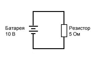
Эта простая схема состоит из батареи и резистора, соединенных напрямую вместе. Нам известно напряжение батареи (10 В) и сопротивление резистора (5 Ом), но больше ничего неизвестно о схеме. Если мы опишем эту схему для SPICE, она сможет сказать нам (по крайней мере), какой ток у нас будет в цепи, используя закон Ома (I=E/R).
SPICE – это программа, использующая текст
SPICE не может напрямую понять диаграмму схемы или любую другую форму графического описания. SPICE – это компьютерная программа, использующая текст, которая требует, чтобы схема была описана относительно ее составляющих компонентов и точек соединений. Каждая уникальная точка соединения в цепи описывается для SPICE номером «узла». Точки, которые являются электрически общими друг для друга в моделируемой цепи, обозначаются одним номером. Возможно, будет полезно думать об этих числах как о номерах «проводов», а не как о номерах «узлов», следуя определению, данному в предыдущем разделе. Так компьютер узнает, что с чем связано: через общие номера проводов или узлов. В схеме из нашего примера есть только два «узла»: верхний провод и нижний провод. SPICE требует, чтобы где-то в цепи был узел 0, поэтому мы обозначим наши провода 0 и 1:
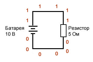
На приведенной выше иллюстрации я показал несколько меток «1» и «0» вокруг каждого провода, чтобы подчеркнуть концепцию общих точек, имеющих общие номера узлов; но всё же это графическое изображение, а не текстовое описание. Прежде чем можно будет продолжить анализ, SPICE должен получить значения компонентов и номера узлов в текстовой форме.
Использование текстового редактора для создания файлов SPICE
Создание текстового файла на компьютере включает использование программы, называемой текстовым редактором. В текстовых редакторах отсутствует возможность форматирования текстовых процессоров (без курсивных, полужирных или подчеркнутых символов), и это хорошо, поскольку такие программы, как SPICE, не знают, что делать с этой дополнительной информацией. Если мы хотим создать простой текстовый файл, в котором абсолютно ничего не записано, кроме символов клавиатуры, мы выбираем, текстовый редактор.
При использовании операционной системы Microsoft, такой как DOS или Windows, с системой идут несколько текстовых редакторов. В DOS есть старая программа редактирования текста Edit, которую можно вызвать, набрав edit в командной строке. В Windows стандартным выбором будет текстовый редактор Notepad. Доступно множество и других программ для редактирования текста. Я использую бесплатный текстовый редактор под названием Vim и запускаю его в операционных системах Windows 95 и Linux. Неважно, какой редактор вы используете, поэтому не беспокойтесь, если скриншоты в этом разделе не похожи на ваши; здесь важна информация о том, что вы вводите, а не о том, какой редактор вы используете.
Примечание: возможно, вам будет удобно использовать редактор Notepad++, для которого есть плагин для подсветки синтаксиса SPICE.
Чтобы описать для SPICE эту простую схему из двух компонентов, я начну с вызова моей программы текстового редактора и ввода строки «названия» для схемы:
Мы можем описать батарею, набрав строку текста, начинающуюся с буквы «v» (означает «voltage source», источник напряжения), указав, к какому проводу подключается каждая клемма батареи (номера узлов), и напряжение батареи, например:
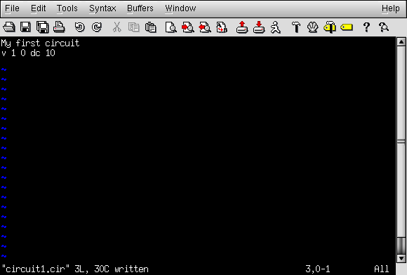
Данная строка сообщает SPICE, что у нас есть источник напряжения, подключенный между узлами 1 и 0, являющийся источником постоянного напряжения (DC), с напряжением 10 вольт. Это всё, что нужно знать компьютеру о батарее.
Теперь обратимся к резистору: SPICE требует, чтобы резисторы были описаны буквой «r», номерами двух узлов (точек соединения) и сопротивлением в омах. Поскольку это компьютерное моделирование, указывать номинальную мощность резистора не нужно. В «виртуальных» компонентах есть одна хорошая черта: им не могут повредить чрезмерное напряжение или ток!
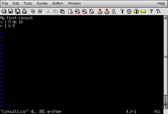
Теперь SPICE будет знать, что между узлами 1 и 0 подключен резистор со значением 5 Ом. Эта очень короткая строка текста сообщает компьютеру, что у нас есть резистор («r»), подключенный между теми же двумя узлами, что и батарея (1 и 0), со значением сопротивления 5 Ом.
Если мы добавим в эту последовательность команд SPICE оператор .end, чтобы указать конец описания схемы, у нас будет вся необходимая SPICE информация, собранная в одном файле и готовая к обработке. Это описание схемы, состоящее из строк в текстовом файле, технически известно как список соединений (netlist или deck):

Перемещение текстовых файлов в SPICE
После того, как мы закончили вводить все необходимые команды SPICE, нам нужно «сохранить» их в файл на жестком диске компьютера, чтобы SPICE мог ссылаться на него при запуске. Поскольку это мой первый список соединений SPICE, я сохраню его под именем «circuit1.cir» (фактическое имя произвольно). Вы можете назвать свой первый список соединений SPICE совершенно другим именем, при условии, что вы не нарушаете никаких правил именования файлов своей операционной системы, например, используя не более 8 + 3 символов (восемь символов в имени и три символа в расширении: 12345678.123) в DOS.
Чтобы вызвать SPICE (указать ему, что необходимо обработать содержимое файла списка соединений circuit1.cir), мы должны выйти из текстового редактора и получить доступ к командной строке, где мы можем ввести текстовые команды для операционной системы компьютера. Этот «примитивный» способ вызова программы может показаться архаичным пользователям компьютеров, привыкшим к графической среде «укажи и щелкни», но это очень мощный и гибкий способ решения задач. Помните, что то, что вы делаете здесь, используя SPICE, является простой формой компьютерного программирования, и чем больше вы будете привыкать давать компьютеру команды в текстовой форме (в отличие от простого щелчка мышью по иконкам), тем большее мастерство в управлении компьютером вы приобретете.
В командной строке введите следующую команду, а затем нажмите клавишу Enter (в этом примере используется имя файла circuit1.cir; если вы выбрали другое имя файла для файла списка соединений, замените его):
spice < circuit1.cirВот как это выглядит на моем компьютере (под управлением операционной системы Linux) непосредственно перед нажатием клавиши Enter:
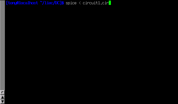
Как только вы нажмете клавишу Enter для выполнения этой команды, на экране компьютера должен будет напечататься текст из вывода SPICE. Ниже приведен скриншот, показывающий, что SPICE вывел на моем компьютере (я увеличил окно «терминала», чтобы показать вам полный текст; в терминале обычного размера текст легко превышает длину одной страницы):
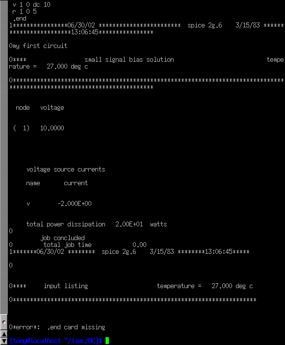
SPICE начинает свой вывод с повторения списка соединений, полностью от строки названия до оператора .end. Примерно на середине моделирования он отображает напряжения во всех узлах относительно узла 0. В этом примере у нас только один узел, кроме узла 0, поэтому он отображает напряжение в нем: 10,0000 вольт. Затем он выводит величину силы тока, протекающего через каждый источник напряжения. Поскольку у нас только один источник напряжения во всей схеме, он отображает только ток через него. В этом случае сила тока через источник составляет 2 ампера. Из-за причуды в способе, которым SPICE анализирует ток, значение 2 ампера выводится как отрицательное: (-) 2 ампера.
Последняя строка в отчете компьютерного анализа – «total power dissipation» (полная рассеиваемая мощность), которая в данном случае выражается как «2.00E+01» ватт: 2.00 x 101, или 20 ватт. SPICE выводит большинство значений в виде экспоненциальной записи, а не в виде обычной записи (с фиксированной запятой). Хотя сначала это может показаться более запутанным, на самом деле эта запись будет проще, когда будут задействованы очень большие или очень маленькие числа. Подробности экспоненциальной записи будут рассмотрены в следующей главе этой книги.
Одним из преимуществ использования «примитивной», использующей текст программы, такой как SPICE, является то, что текстовые файлы, с которыми мы имеем дело, чрезвычайно малы по сравнению с другими форматами файлов, особенно графическими форматами, используемыми в другом программном обеспечении для моделирования схем. Кроме того, тот факт, что вывод SPICE представляет собой обычный текст, означает, что вы можете направить вывод SPICE в другой текстовый файл, где он может быть обработан. Для этого мы повторно отправляем команду операционной системе компьютера, чтобы запустить SPICE, на этот раз перенаправляя вывод в файл, который я назову «output.txt»:
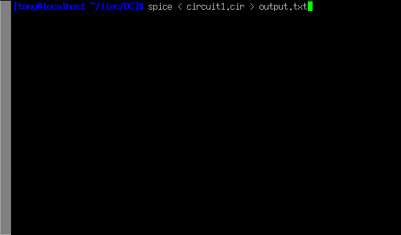
На этот раз SPICE будет работать «тихо», без вывода текстового потока на экран компьютера, как раньше. Будет создан новый файл output1.txt, который вы можете открыть и изменить с помощью текстового редактора. Для иллюстрации этого я воспользуюсь тем же текстовым редактором (Vim) и открою этот файл результатов:
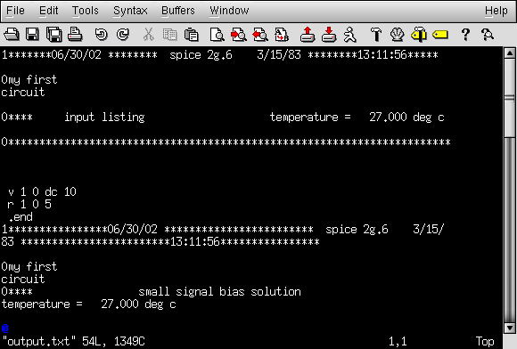
Теперь я могу свободно редактировать этот файл, удаляя любой посторонний текст (например, «баннеры», показывающие дату и время), оставляя только текст, который, как мне кажется, имеет отношение к анализу моей схемы:
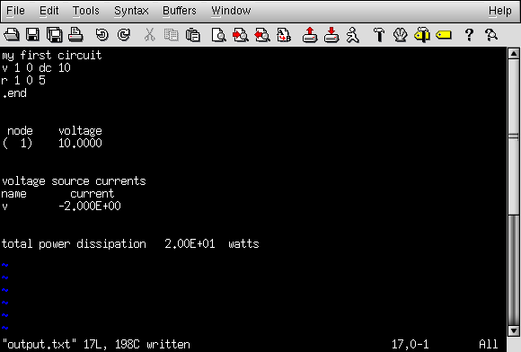
После соответствующего редактирования и повторного сохранения под тем же именем файла (в этом примере output.txt) текст может быть вставлен в любой документ, причем «простой текст» является универсальным форматом файла почти для всех компьютерных систем. Я даже могу включить его прямо в текст этой книги, вместо графического изображения «скриншота», например:
my first circuit
v 1 0 dc 10
r 1 0 5
.end
node voltage
( 1) 10.0000
voltage source currents
name current
v -2.000E+00
total power dissipation 2.00E+01 watts
Кстати, этот формат для вывода текста из моделирования SPICE в этой серии книг является предпочтительным: в виде текста, а не в виде картинок скриншотов.
Изменение значений в SPICE
Чтобы изменить значение компонента в моделировании, нам нужно открыть файл списка соединений (circuit1.cir) и внести необходимые изменения в текстовое описание схемы, затем сохранить эти изменения в файле с тем же именем и повторно запустить SPICE через командную строку. Этот процесс редактирования и обработки текстового файла знаком каждому программисту. Одна из причин, по которой мне нравится преподавать SPICE, заключается в том, что он подготавливает студента к тому, чтобы думать и работать как программист, и это хорошо, потому что программирование – это важная область работы, связанная с передовой электроникой.
Ранее мы исследовали последствия изменения одной из трех переменных в электрической цепи (напряжения, тока или сопротивления), используя закон Ома, чтобы математически предсказать, что произойдет. Теперь давайте попробуем сделать то же самое с помощью SPICE, чтобы он выполнил вычисления за нас.
Если бы мы утроили напряжение в схеме из нашего последнего примера с 10 до 30 вольт и оставили сопротивление цепи неизменным, мы бы ожидали, что ток также утроится. Давайте попробуем выполнить это, изменив имя нашего файла списка соединений, чтобы не перезаписывать первый файл. Таким образом, оба варианта моделирования схемы будут храниться на жестком диске нашего компьютера для будущего использования. Результатом работы SPICE для этого измененного списка соединений будет следующий текстовый список:
second example circuit
v 1 0 dc 30
r 1 0 5
.end
node voltage
( 1) 30.0000
voltage source currents
name current
v -6.000E+00
total power dissipation 1.80E+02 watts
Как мы и ожидали, ток утроился с увеличением напряжения. Раньше ток составлял 2 ампера, но теперь он увеличился до 6 ампер (-6,000 x 100). Также обратите внимание, как увеличилась общая рассеиваемая мощность в цепи. Раньше она составлял 20 Вт, а сейчас 180 Вт (1,8 x 10²). Если вспомнить, что мощность пропорциональна квадрату напряжения (закон Джоуля: P=E2/R), то этого можно было ожидать. Если мы утроим напряжение в цепи, мощность должна увеличиться в девять раз (32 = 9). Результат произведения 9 и 20 действительно равен 180, поэтому выходные данные SPICE действительно коррелируют с тем, что мы знаем о мощности в электрических цепях.
Создание комментариев в SPICE
Если мы хотим увидеть, как эта простая схема будет реагировать на широкий диапазон напряжений батареи, мы можем задействовать некоторые из более продвинутых опций SPICE. Здесь я воспользуюсь опцией анализа «.dc«, чтобы изменять напряжение батареи от 0 до 100 вольт с шагом 5 вольт, выводя на каждом этапе напряжение и силу тока в цепи. Строки в списке соединений SPICE, начинающиеся со звездочки («*«), – это комментарии. То есть они не заставляют компьютер делать что-либо, связанное с анализом схемы, а служат просто заметками для любого человека, читающего текст списка соединений.
third example circuit
v 1 0
r 1 0 5
*оператор ".dc" говорит spice пройтись напряжением
*источника "v" от 0 до 100 вольт шагом 5 вольт.
.dc v 0 100 5
.print dc v(1) i(v)
.end
Команды печати и вывода графиков
Команда .print в этом списке соединений SPICE инструктирует SPICE напечатать таблицу чисел, в которой каждая строка соответствует отдельному этапу анализа:
v             i(v)
0.000E+00     0.000E+00
5.000E+00    -1.000E+00
1.000E+01    -2.000E+00
1.500E+01    -3.000E+00
2.000E+01    -4.000E+00
2.500E+01    -5.000E+00
3.000E+01    -6.000E+00
3.500E+01    -7.000E+00
4.000E+01    -8.000E+00
4.500E+01    -9.000E+00
5.000E+01    -1.000E+01
5.500E+01    -1.100E+01
6.000E+01    -1.200E+01
6.500E+01    -1.300E+01
7.000E+01    -1.400E+01
7.500E+01    -1.500E+01
8.000E+01    -1.600E+01
8.500E+01    -1.700E+01
9.000E+01    -1.800E+01
9.500E+01    -1.900E+01
1.000E+02    -2.000E+01
Если я повторно отредактирую файл списка соединений, заменив команду .print на команду .plot, SPICE выведет грубый график, состоящий из текстовых символов:
Legend:  + = v#branch
------------------------------------------------------------------------
sweep      v#branch-2.00e+01             -1.00e+01                 0.00e+00
---------------------|------------------------|------------------------|
0.000e+00  0.000e+00 .                        .                        +
5.000e+00 -1.000e+00 .                        .                     +  .
1.000e+01 -2.000e+00 .                        .                   +    .
1.500e+01 -3.000e+00 .                        .                +       .
2.000e+01 -4.000e+00 .                        .              +         .
2.500e+01 -5.000e+00 .                        .           +            .
3.000e+01 -6.000e+00 .                        .         +              .
3.500e+01 -7.000e+00 .                        .      +                 .
4.000e+01 -8.000e+00 .                        .    +                   .
4.500e+01 -9.000e+00 .                        . +                      .
5.000e+01 -1.000e+01 .                        +                        .
5.500e+01 -1.100e+01 .                     +  .                        .
6.000e+01 -1.200e+01 .                   +    .                        .
6.500e+01 -1.300e+01 .                +       .                        .
7.000e+01 -1.400e+01 .              +         .                        .
7.500e+01 -1.500e+01 .           +            .                        .
8.000e+01 -1.600e+01 .         +              .                        .
8.500e+01 -1.700e+01 .      +                 .                        .
9.000e+01 -1.800e+01 .    +                   .                        .
9.500e+01 -1.900e+01 . +                      .                        .
1.000e+02 -2.000e+01 +                        .                        .
---------------------|------------------------|------------------------|
sweep      v#branch-2.00e+01             -1.00e+01                 0.00e+00
В обоих выходных форматах левый столбец чисел представляет напряжение батареи на каждом этапе, и по нему видно, что оно увеличивается от 0 до 100 вольт, по 5 вольт за раз. Числа в правом столбце указывают силу тока в цепи для каждого из этих напряжений. Посмотрите внимательно на эти числа, и вы увидите пропорциональную связь в каждой паре значений: закон Ома (I=E/R) верен в каждом случае, каждое значение силы тока составляет 1/5 соответствующего значения напряжения, потому что сопротивление цепи составляет ровно 5 Ом. Опять же, отрицательные числа для силы тока в данном анализе SPICE – это скорее причуда, чем что-либо еще. Просто обращайте внимание на абсолютное значение каждого числа, если не указано иное.
Программы для интерпретации и преобразования данных SPICE
Существуют даже некоторые программы, способные интерпретировать и преобразовывать неграфические данные, выводимые SPICE, в графические диаграммы. Одна из этих программ называется Nutmeg, и ее выходные данные выглядят примерно так:
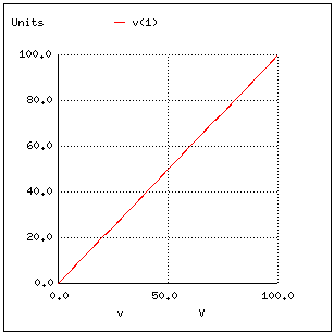
Обратите внимание, как Nutmeg выводит график напряжения на резисторе v(1) (напряжение между узлом 1 и предполагаемой опорной точкой узла 0) в виде линии с положительным наклоном (от нижнего левого к верхнему правому углу). Станете ли вы когда-нибудь опытным в использовании SPICE, не имеет отношения к его применению в данной книге. Важно только то, чтобы вы поняли, что означают числа в отчете, созданном SPICE. В следующих примерах я приложу все усилия, чтобы аннотировать численные результаты SPICE, чтобы устранить любую путаницу и раскрыть всю мощь этого удивительного инструмента, который поможет вам понять поведение электрических цепей.
Программный пакет LTspice
В качестве альтернативы консольному симулятору SPICE можно рассмотреть использование программного обеспечения LTspice от Analog Devices. LTspice представляет собой мощный программный пакет, включающий в себя SPICE-симулятор, редактор принципиальных схем и средство просмотра осциллограмм с улучшениями и моделями, позволяющими упростить моделирование аналоговых схем.
Основы работы с LTspice представлены в следующих статьях:
- Основы моделирования схем в LTSpice
- Руководство по LTSpice (средний уровень)
А ниже показаны скриншоты примера схемы и ее анализа.
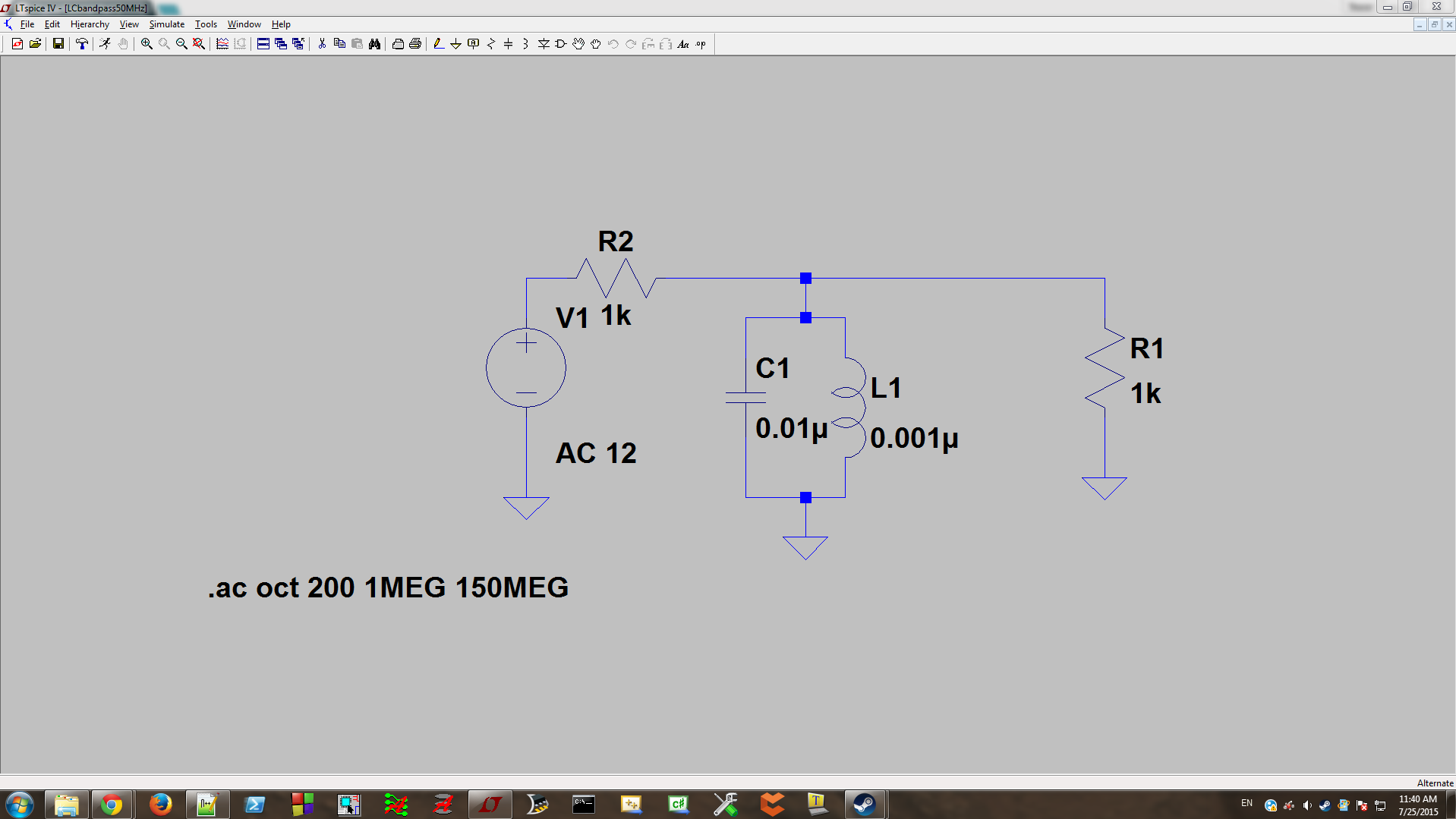
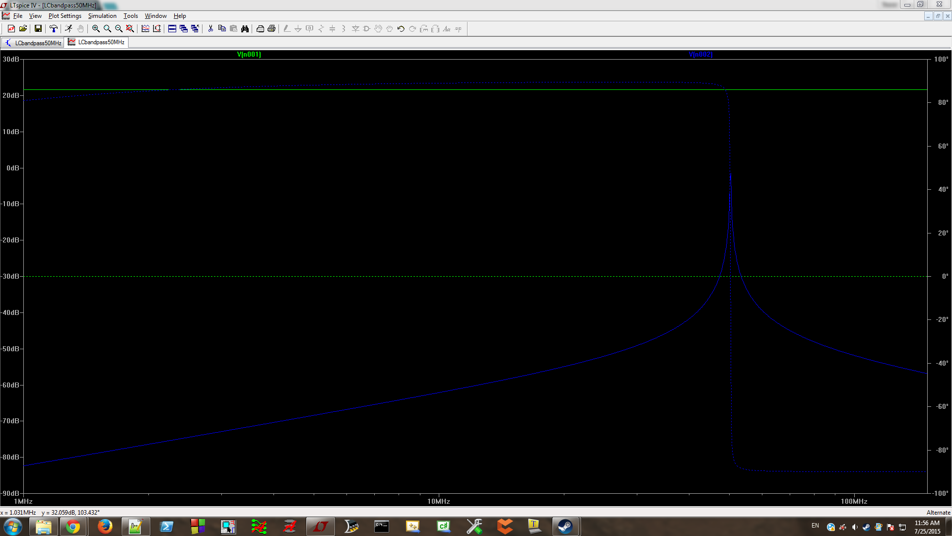
Теги
LTspiceSPICEМоделированиеОбучениеСхемотехника
Коротко о SPICE
В настоящее время наибольшую популярность имеют программы, использующие SPICE (Simulation Program with Integrated Circuit Emphasis) алгоритм моделирования процессов, протекающих в электронных схемах. Алгоритм SPICE, разработанный в конце 1970-х годов в университете Беркли (Калифорния), де-факто стал стандартом для разрабатываемых и уже эксплуатируемых в настоящее время коммерческих систем схемотехнического моделирования для персонального компьютера. К таким системам относятся: HSPICE (фирма MetaSoftware), PSpice (Microsim), MicroCap (Spectrum Software), Circuit Maker (The Virtual Elektronics Lab), Dr. Spice, ViewSpice (Deutsch Research) и другие. Учитывая тот факт, что не все могут приобрести коммерческую систему схемотехнического моделирования, остановим свой выбор на бесплатном симуляторе LTspice IV (далее просто LTspice) от корпорации Linear Technology (www.linear.com). Программа может работать под управлением ОС Windows 98, 2000, NT4.0, Me или XP. Кроме того, LTspice тестировался под Linux RedHat 8.0 с WINE версии 20030219.
LTspice был первоначально основан на симуляторе аналоговых схем SPICE 3F4/5, свободно доступной версии симулятора SPICE. С момента своего создания LTspice подвергался постоянным изменениям с целью его улучшения, устранения ошибок и расширения возможностей. Современная версия LTspice представляет собой превосходный симулятор, позволяющий моделировать аналоговые, цифровые, а также смешанные схемы.
LTspice отличается очень понятным и дружественным интерфейсом, позволяющим даже новичку очень быстро научиться работать с ним. Новые схемы можно разрабатывать с помощью встроенного редактора схем. Директивы и параметры симулятора помещаются прямо на схеме с использованием стандартного SPICE-синтаксиса. Диаграммы напряжений и токов в узлах и ветвях схемы могут быть получены простым щелчком левой кнопки мышки по соответствующей точке схемы.
LTspice имеет отличный (правда, англоязычный) встроенный помощник Help [1], который является как описанием этой программы, так и руководством для работы с ней. В Интернете существует много ресурсов, где обсуждается и поддерживается эта программа [2].
Необходимость пополнения библиотеки моделей
Симулятор LTspice изначально предназначался для демонстрационного моделирования импульсных источников питания, использующих управляющие микросхемы производства Linear Technology. При этом LTspice демонстрирует приличную скорость моделирования и оптимальную совместимость с другими стандартами SPICE, что позволяет непосредственно использовать или легко адаптировать к нему оригинальные SPICE-модели различных производителей. Последнее обстоятельство весьма важно, так как на каком-то этапе работы с SPICE-симулятором каждый пользователь сталкивается с необходимостью пополнения библиотеки моделей. К радости пользователей симулятора LTspice можем сообщить, что проблема пополнения встроенной библиотеки новыми моделями уже в значительной степени решена поколениями энтузиастов, работающих с этой программой. Много дополнительных моделей можно найти в файловом архиве независимой пользовательской группы программы LTspice/SwitcherCAD III [3]. Кроме того, следует посетить небольшую, но весьма информативную домашнюю страничку Андрея Кадатча [4] и скачать дополнительную библиотеку EXTRA, которая выводит объем библиотеки LTspice на уровень, сравнимый с библиотеками коммерческих симуляторов.
К сожалению, даже пополненная библиотека не гарантирует того, что в какой-то момент под рукой окажется необходимая модель. Во многих коммерческих SPICE-симуляторах присутствуют специальные утилиты, позволяющие рассчитывать параметры стандартных моделей по справочным данным реальных компонентов. Разумеется, в бесплатной программе подобная утилита отсутствует, однако это не мешает пользователям LTspice воспользоваться результатами расчета сторонней программы. Практически все производители электронных компонентов выкладывают соответствующие SPICE-модели этих компонентов на своих интернет-сайтах. Обычно эти модели выполнены в виде подсхем. Остается только корректно пополнить этими моделями существующую библиотеку. Если используется стандартная модель, то процесс пополнения простой и выполняется без особых проблем. Если же используется модель в виде подсхемы, то пополнение усложняется и не всегда может закончиться успешно. Рассмотрим оба этих варианта.
Пополнение библиотеки схемными элементами, имеющими стандартную модель
Параметры схемных элементов, имеющих стандартные модели, расположены в подкаталоге /lib/cmp относительно корневого каталога программы. Здесь можно обнаружить следующие файлы:
- standard.bjt — библиотека моделей биполярных транзисторов;
- standard.cap — библиотека моделей конденсаторов;
- standard.dio — библиотека моделей диодов;
- standard.ind — библиотека моделей индуктивностей;
- standard.jft — библиотека моделей полевых транзисторов с управляющим p—n-переходом (JFET);
- standard.mos — библиотека моделей полевых транзисторов с изолированным затвором (MOSFET).
Каждая строка в этих файлах, кроме standard. cap и standard.ind, представляет собой соответствующую директиву .model. Следовательно, пополнение этих библиотек можно осуществить простым вписыванием очередной директивы .model с соответствующими параметрами. Например, дополним библиотеку биполярных транзисторов моделью отечественного транзистора типа КТ315А:
.model kt315a NPN (Is=2.82f Xti=3 Eg=1.11 Vaf=3.32K Bf=55 Ne=2.35
Ise=554.1p Ikf=18.04m Xtb=1.5
+ Br=.6455 Nc=2 Isc=0 Ikr=0 Rc=0 Cjc=17p Vjc=.75 Mjc=.333 Fc=.5
Cje=8.55p Vje=.75 Mje=.333
+ Tr=3.36u Tf=1.02n Itf=0 Vtf=0 Xtf=0 Vceo=25 Icrating=100m
mfg=USSR)
После дополнения библиотечного файла транзистор KT315A становится доступным для использования (рис. 1).Последние три параметра Vceo, Icrating, mfg=USSR в моделировании не участвуют, но, соответственно, позволяют вывести в строке выбора транзистора его максимальное напряжение коллектор-эмиттер, ток коллектора и наименование производителя.

Рис. 1. Выбор биполярного транзистора КТ315А из библиотеки LTspice
Пополнение библиотеки схемными элементами, имеющими модель в виде подсхемы
Если модель существует в виде подсхемы, то в этом случае придется решить, как минимум, две задачи. Во-первых, надо создать новый или подобрать готовый символ для будущего библиотечного элемента. Во-вторых, надо согласовать SPICE-синтаксис, используемый при описании модели, с синтаксисом LTspice.
Например, пополним библиотеку отечественным операционным усилителем типа К544УД2 (рис. 2).

Рис. 2. Схема включения операционного усилителя К544УД2
Приведем текст подсхемы модели этого операционного усилителя:
| * k544ud2 operational amplifier “macromodel” subcircuit * created using Parts version 1.04 on 10/11/90 at 10:58 * |
||
| * connections: * * * * * * .subckt k544ud2 * |
non-inverting input | inverting input | | positive power supply | | | negative power supply | | | | output | | | | | compensation | | | | | / 1 2 3 4 5 6 7 |
|
| c1 dc de dlp dln dp egnd fb ga gcm iss hlim j1 j2 r2 rd1 rd2 ro1 ro2 rp rss vb vc ve vlim vlp vln |
11 12 174.6E-15 5 53 dx 54 5 dx 90 91 dx 92 90 dx 4 3 dx 99 0 poly(2) (3,0) (4,0) 0 .5 .5 7 99 poly(5) vb vc ve vlp vln 0 127.3E6 -100E6 100E6 100E6 -100E6 6 0 11 12 1.885E-3 0 6 10 99 188.5E-9 3 10 dc 400.0E-6 90 0 vlim 1K 11 2 10 jx 12 1 10 jx 6 9 100.0E3 4 11 530.5 4 12 530.5 8 5 50 7 99 25 3 4 9.000E3 10 99 500.0E3 9 0 dc 0 3 53 dc 2 54 4 dc 2 7 8 dc 0 91 0 dc 20 0 92 dc 20 |
|
| .model dx D(Is=800.0E-18) .model jx PJF(Is=15.00E-12 Beta=17.77E-3 Vto=-1) .ends |
Синтаксис различных SPICE-симуляторов может иметь различия. Поэтому, если подсхема модели заимствована у другого симулятора или взята с сайта производителя электронных компонентов, необходимо внимательно просмотреть ее текст, чтобы выявить и ликвидировать синтаксические несоответствия.
Сравнив нумерацию выводов реального операционного усилителя (рис. 2) и порядок узлов в строке директивы “.subckt k544ud2 1 2 3 4 5 6 7”, можно заметить их несоответствие. Соответствие нумерации и порядка узлов подсхемы может потребоваться, если схемный редактор LTspice используется как генератор списка связей для сторонней программы, например, предназначенной для разводки печатной платы. В данном случае такая задача не ставится, и поэтому для нормального функционирования модели достаточно лишь обеспечить верный порядок передачи узловых потенциалов из основной схемы в подсхему, без привязки к физической реализации самой микросхемы.
Так как операционный усилитель является стандартным электронным узлом, то найти для него готовый символ скорей всего не составит труда. И в самом деле, требуемый символ можно позаимствовать у операционного усилителя LT1008, который расположен в подкаталоге Opamps встроенной библиотеки (рис. 3).

Рис. 3. Поиск подходящего символа во встроенной библиотеке программы LTspice
Чтобы использовать готовый символ, мы должны знать порядок, в котором он передает узлы в подсхему модели. Этот порядок можно узнать, воспользовавшись редактором символов программы LTspice, который будет далее рассмотрен подробно, а пока постараемся решить эту проблему при помощи схемного редактора. Для этого, воспользовавшись командой Edit=>Component или нажав клавишу F2, загрузим символ требуемого операционного усилителя из раздела Opamps встроенной библиотеки и разместим его в рабочем поле схемного редактора. Далее, воспользовавшись командой Edit=>Draw Wire или нажав клавишу F3, подключаем к выводам операционного усилителя короткие фрагменты внешних цепей и принудительно присваиваем им имена, соответствующие порядку перечисления узлов в строке директивы .subckt подсхемы модели операционного усилителя К544УД2 (рис. 4).

Рис. 4. Присвоение имен внешним цепям символа операционного усилителя LT1008
Чтобы присвоить имя цепи, нужно вызвать соответствующее меню операций, щелкнув по требуемой цепи правой кнопкой мышки. В появившемся меню выбрать режим Label Net («Ярлык для цепи»), что позволит получить доступ к меню Net Name («Имя цепи»), где в строке ABC присваивается требуемое имя (рис. 4).
Воспользовавшись командой View=>SPICE Netlist, посмотрим список связей нашей небольшой схемы (рис. 5) и убедимся, что порядок узлов в строке “XU1 1 2 3 4 5 6 7 LT1008” соответствует порядку узлов в строке “.subckt k544ud2 1 2 3 4 5 6 7”. В противном случае необходимо соответствующим образом отредактировать строку директивы .subckt.

Рис. 5. Проверка порядка узлов, передаваемого символом LT1008 в подсхему модели
Программа LTspice регулярно обновляется через Интернет. Поэтому, чтобы не потерять свои библиотеки, желательно выделить их в свою пользовательскую папку. Чтобы папка была видна при выборе нового компонента, ее необходимо разместить в подкаталоге sym встроенной библиотеки. Присвоим этот папке имя Mylib. Создадим в этой папке файл r-opamp.lib и скопируем туда вышеуказанный текст подсхемы модели. Впоследствии этот файл можно пополнять другими моделями операционных усилителей отечественного производства. В начале файла, в виде комментариев, необходимо сделать небольшую информационную вставку, описывающую содержимое библиотеки. Это облегчит работу с библиотекой, а также позволит избежать каких-то досадных ошибок.
Пример информационной вставки:
*******************************************************************
* Библиотека моделей операционных усилителей
* отечественного производства
*
*******************************************************************
*
* Библиотека сoдержит:
* К544УД2
*
*******************************************************************
* Внимание! Нумерация (порядок) входных узлов подсхем
* моделей всех ОУ не совпадает с реальной нумерацией выводов
* корпуса микросхем.
*******************************************************************
Примечание. Для схемных элементов различных типов лучше создавать независимые библиотечные файлы. Например, для ШИМ-контроллеров можно создать файл pwm.lib, для полевых транзисторов с изолированным затвором—mosfet.lib и т. д.
Скопируем файл символа LT1008.asy из своего каталога ..libsymOpamps в пользовательский каталог ..libsym Mylib и переименуем его в k544ud2.asy. Однако одного переименования недостаточно. Необходимо также внести некоторые изменения и в сам файл. Для этого откроем его при помощи любого текстового редактора и изменим содержимое атрибутов SYMATR:
SYMATTR Value — вместо LT1008 записываем k544ud2
SYMATTR Prefix X— оставляем без изменения
SYMATTR SpiceModel — вместо LTC.lib записываем r-opamp.lib
SYMATTR Value2 — вместо LT1008 записываем k544ud2
SYMATTR Description — запишем Operational Amplifier
После этого сохраним изменения и приступим к испытанию. Для этого запустим программу LTspice в режиме схемного редактора и проверим наличие нового электронного компонента в библиотеке. Если все сделано правильно, то операционный усилитель К544УД2 можно обнаружить именно там, где он и должен быть, то есть в пользовательском каталоге Mylib (рис. 6).

Рис. 6. Выбор операционного усилителя К544УД2 из библиотеки пользователя
Для проверки функционирования схемного элемента можно собрать какую-то тестовую схему. Пусть такой схемой будет обычный инвертирующий усилитель (рис. 7).

Рис. 7. Тестовая схема инвертирующего усилителя на ОУ К544УД2
Согласно результатам моделирования, модель операционного усилителя К544УД2 функциональна, и инвертирующий усилитель, собранный на нем, обеспечивает заданное усиление Kу = R3/R2 = 100к/10к =10.
Создание модели схемного элемента с использованием иерархической схемы
Ранее мы рассмотрели случаи создания схемного элемента, когда его модель уже существует в том или ином виде. Обычно так и происходит, но иногда бывают ситуации, когда модели нет, и ее невозможно найти ни в одном из доступных информационных источников. В этом случае приходится создавать схемный элемент с нуля. Обычно создание нового элемента начинается с создания его модели.
В качестве примера, используя средства программы LTspice, создадим модель микросхемы TL494. Микросхема TL494 является ШИМ-контроллером импульсного источника питания и включает в себя все необходимые для этого блоки. Эта микросхема, благодаря своим достаточно высоким характеристикам и низкой стоимости, очень популярна как среди любителей, так и среди профессионалов в силовой электронике. Так же как и широко известный 555-й таймер, TL494 выпускают многие мировые производители электронных компонентов, такие как Texas Instruments, ON Semiconductor, Motorola, Fairchild Semiconductor, Fujitsu, Samsung и т. д. Эта микросхема выпускается под своим оригинальным, а также под альтернативными названиями, такими как mPC494C, MB3759, KA7500B, IR3M02 и т. п. Отечественной версией TL494 является микросхема 1114ЕУ4.
Однако, несмотря на популярность, модель TL494 пока отсутствует в библиотеках коммерческих симуляторов и на сайтах производителей электронных компонентов.
Иерархические схемы
В программе LTspice предусмотрена очень полезная возможность замены отдельных фрагментов схемы схемами с более низким уровнем иерархии. Причем, в основной схеме, имеющей высокий уровень, эти иерархические схемы выглядят как абстрактные символы с выводами. В этом смысле иерархические схемы, по сути, очень похожи на подсхемы, но гораздо удобнее и нагляднее, так как пользователю приходится работать не с текстовым файлом, а с реальной схемой. Ее легко изменить и контролировать обычными средствами схемного редактора программы LTspice.
Так же как и подсхемы, иерархические схемы могут быть помещены в библиотеку для последующего использования в различных проектах. Но, в отличие от подсхем, ссылаться на иерархическую схему из основного проекта можно только с помощью символа. Файл символа должен иметь такое же имя, что и файл иерархической схемы. Например, если файл иерархической схемы имеет название tl494h.asc, то файл символа должен иметь название tl494h.asy. По этой же причине имя символа не должно содержать пробелы, а также символы, недопустимые для имени файла.
Примечание. Иерархическая схема должна располагаться в одном каталоге с основной схемой.
Имена выводов символов должны соответствовать именам соответствующих цепей иерархической схемы. Таким образом, создается связь между основной и иерархическими схемами.
Любой файл, открытый с помощью команды File=>Open, рассматривается как схема высокого уровня.
Создание модели TL494 в виде иерархической схемы
Справочную информацию о микросхеме TL494 можно взять, например, на сайте компаний Texas Instruments [5] или ON Semiconductor [6].
На рис. 8 изображена ее функциональная схема.

Рис. 8. Функциональная схема TL494
Казалось бы, что для создания корректной модели достаточно найти и продублировать принципиальную электрическую схему TL494. Благо, упрощенные версии отдельных узлов даже приводятся в документации, расположенной на сайте Texas Instruments [7]. Однако попытка создания модели таким способом скорей всего закончится неудачей. Дело в том, что, несмотря на свои маленькие размеры, микросхема имеет достаточно сложную электрическую принципиальную схему, содержащую более 50 транзисторов. Модель, содержащая такое количество активных элементов, способна в значительной мере снизить скорость симуляции или сделать ее вообще невозможной из-за проблем сходимости. Выход из данной ситуации — использование встроенных схемных элементов LTspice, которые являются функциональными аналогами отдельных узлов моделируемой микросхемы.
Генератор
ШИМ-контроллер TL494 работает на фиксированной частоте, которая определяется внутренним генератором. Частота генератора программируется внешними резистором и конденсатором, подключаемыми к выводам Rт и Cт микросхемы. Конденсатор Cт заряжается стабильным током, величина которого задается с помощью резистора Rт. После того, как напряжение на конденсаторе достигает 3 В, он быстро разряжается до нуля, и процесс снова повторяется. Величину зарядного тока можно определить по формуле Iзар ≈ 3,65/Rт. На рис. 9 приведены графические зависимости частоты внутреннего генератора от номиналов частотозадающих элементов. Эту частоту также можно определить по формуле Fген = 1,2/(RT·CT).

Рис. 9. Частота генератора и ее температурный дрейф в зависимости от величин Rт и Cт
Схема модели генератора изображена на рис. 10.

Рис. 10. Схема модели задающего генератора
Источник напряжения V1 имитирует напряжение, приложенное к резистору Rт. ИТУТ (источника тока, управляемый током) F1 является своеобразным токовым зеркалом, которое формирует ток зарядки конденсатора Cт, равный току, протекающему через источник напряжения V1 и резистор Rт. Под воздействием этого тока конденсатор Cт линейно заряжается. Как только напряжение на конденсаторе достигает порогового напряжения 3 В, он разряжается с помощью ключа S1. Диод D1 предотвращает обратный ток и позволяет напряжению на выводе Rт подниматься выше потенциала источника напряжения V1.
При указанных на схеме номиналах резистора Rт = 12 кОм и конденсатора Cт = 10 мкФ рабочая частота генератора составляет 10 кГц, что соответствует графической зависимости на рис. 9.
Усилитель ошибки
Регулировочные характеристики ШИМ-контроллера определяются амплитудно-частотной характеристикой (АЧХ) его усилителя ошибки. Поэтому при создании модели усилителя нужно обеспечить корректность этой характеристики. Согласно документации Texas Instruments и других производителей, АЧХ усилителя ошибки имеет частоту среза 10 Гц с последующим завалом 20 дБ/дек (рис. 11).

Рис. 11. Амплитудно-частотная характеристика усилителя ошибки
Подобную АЧХ можно легко получить с помощью RC-фильтра нижних частот. Схема модели усилителя ошибки с RC-фильтром нижних частот, а также результаты моделирования изображены на рис. 12.

Рис. 12. Модель усилителя ошибки
Фильтр нижних частот R1, C1 позволяет получить АЧХ, которая идеально совпадает с изображенной на рис. 11.
Нелинейность передаточной характеристики усилителя ошибки, а также коэффициент усиления на низких частотах имитируются с помощью ИНУН (источник напряжения, управляемый напряжением) E1. Согласно общим справочным данным на ШИМ-контроллер TL494 (документация t1494.pdf и TL494-D.PDF), коэффициент передачи усилителя ошибки AVOL = 50 000 (95 дБ). Коэффициент усиления и передаточную характеристику усилителя ошибки представим в виде таблицы “table=(0,0 1.96m,0 2m,2 2.04m,4 20m,4.5)”.
Источник напряжения V2 определяет рабочую точку усилителя ошибки, а резистор R3 играет роль его нагрузки во время AC-анализа.
Выходной каскад
Выходной каскад контроллера TL494 представляют собой транзистор с открытыми эмиттером и коллектором. Благодаря этому, возможны два варианта включения этого транзистора, где он включен по схеме с общим эмиттером (рис. 13а) или общим коллектором (рис. 13б). Каждому из этих включений соответствует своя зависимость напряжения открытого транзистора Vкэ.нас от тока нагрузки.

Рис. 13. Характеристики напряжения насыщения транзистора выходной схемы для включения: а) с общим эмиттером; б) с общим коллектором
Желательно, чтобы модель корректно имитировала эти характеристики насыщения, а также ситуации превышения максимального тока и пробоя повышенным напряжением транзистора выходного каскада.
Сначала рассмотрим модель выходного каскада, включенного по схеме с общим эмиттером, изображенную на рис. 14.

Рис. 14. Модель выходного каскада, включенного по схеме с общим эмиттером
С помощью ИТУН G1 и стабилитрона D1 имитируется открытый транзистор выходного каскада. Этот эквивалентный транзистор полностью открыт, если ток нагрузки I1 не превышает максимально допустимого значения в 250 мА (для микросхемы TL494 производства Texas Instruments). При превышении максимального тока эквивалентный транзистор насыщается, и напряжение на его выводах резко возрастает (участок 3 ВАХ). В области малых токов (участок 1) ВАХ эквивалентного транзистора определяется внутренним сопротивлением Ron диода D3, а в области средних токов (участок 2) — внутренним сопротивлением параллельно включенных диодов D2 и D3. Пробой эквивалентного транзистора при повышенном напряжении имитируется стабилитроном D1, имеющим напряжение стабилизации Vrev = 41 В. ИТУН G2 в данном режиме не активен, так как напряжение управления всегда равно напряжению питания микросхемы.
Теперь рассмотрим модель выходного каскада, включенного по схеме с общим коллектором, изображенную на рис. 15.

Рис. 15. Модель выходного каскада, включенного по схеме с общим коллектором
В схеме с общим коллектором ИТУН G2 контролирует напряжение на открытом транзисторе выходного каскада. Коэффициент передачи G2 описывается таблицей “table=(0 250m,1.42 243m,1.46 150m,1.57 0)”. Согласно этой таблице, если входное напряжение ИТУН G2 падает ниже 1,57 В, последний начинает шунтировать выход ИТУН G1. Следствием этого шунтирования будет сдвиг ВАХ открытого транзистора в сторону больших напряжений.
Потребляемый ток и источник опорного напряжения
Ток Icc, потребляемый микросхемой TL494, имеет нелинейную зависимость от питающего напряжения Vcc. Эта зависимость изображена на рис. 16.

Рис. 16. Зависимость тока, потребляемого микросхемой TL494, от питающего напряжения
На рис. 17 изображена модель, которая с помощью ИТУН G1 имитирует потребляемый ток микросхемы. Коэффициент передачи ИТУН задан таблицей “table=(1 0,5 4.5m, 6.85 7.6m,40 8.4m)”. Источник опорного напряжения имитируется при помощи источника тока I1 и стабилитрона D1. Ток нагрузки источника опорного напряжения, при помощи поведенческого источника тока B1, суммируется к току, потребляемому микросхемой. В соответствии со справочными данными, ток короткого замыкания источника опорного напряжения составляет 25 мА.

Рис. 17. Модель источника опорного напряжения и имитатора потребляемого тока
Общая схема модели микросхемы TL494
После того, как созданы основные узлы модели, создание общей схемы модели (рис. 18) не вызывает особых затруднений.

Рис. 18. Иерархическая схема модели микросхемы TL494

Рис. 19. Указание наименования и направления цепей
Всем внешним цепям иерархической схемы необходимо присвоить имена. Удобнее всего использовать имена соответствующих выводов микросхемы прототипа. Чтобы присвоить имя цепи, нужно вызвать соответствующее меню операций, щелкнув по требуемой цепи правой кнопкой мышки. В появившемся меню выбрать режим Label Net («Ярлык для цепи»), что позволит получить доступ к меню Net Name («Имя цепи»), где в строке ABC указывается требуемое имя (рис. 19). Для большей наглядности можно определить направления сигнала во внешних цепях с помощью указателя Port type:
- None — без направления;
- Input — входная цепь;
- Output — выходная цепь;
- Bi-Direct — двунаправленная цепь.
Указатель Port type на процессы моделирования не влияет.
Общий провод внутри иерархической схемы лучше не подключать к «земле», а соединить явно или подключить к цепи “COM”. Это позволит в дальнейшем использовать модель в схемах с плавающим, относительно «земли», питанием.
При помощи команды File=>Save As… назовем как TL494H.asc и сохраним в пользовательский каталог ..libsym Mylib полученную иерархическую схему модели TL494.
Редактор символов
Каждый схемный элемент имеет собственный символ, позволяющий легко идентифицировать его на электрической принципиальной схеме. Внешний вид символов схемных элементов, таких как резисторы, конденсаторы, индуктивности, диоды, транзисторы и т. п., оговаривается соответствующим стандартом на конструкторскую документацию. В настоящее время в мире существует два основных стандарта, один из которых американский, а другой — европейский. К последнему весьма близка отечественная «Единая система конструкторской документации» (ЕСКД). В библиотеках LTspice использован американский стандарт на символы схемных элементов. С этим можно смириться, так как обычно данный симулятор не используется для подготовки конструкторской документации, но при необходимости символы схемных элементов можно привести к более привычному виду.
Окно редактора символов
В LTspice имеется специальный редактор символов, с помощью которого можно изменять существующие или создавать новые символы схемных элементов. Для запуска этого редактора необходимо активизировать команду File=>New Symbol. В результате появится окно редактора символов (рис. 20).

Рис. 20. Окно редактора символов
Отличительный признак этого окна — крестик с кружком в центре рабочего поля, а также синий символ логического вентиля ![]() в левой части панели команд.
в левой части панели команд.
Панель команд редактора символов
Панель меню команд очень похожа на аналогичную панель схемного редактора. В отличие от панели команд схемного редактора здесь присутствует меню Draw, но зато отсутствует меню Simulate.
Рассмотрим подробнее подпункты меню команд:
- File — подпункты этого меню аналогичны подпунктам меню File схемного редактора.
- Edit — служит для редактирования символа и содержит следующие подпункты:
- Undo (F9) — отменить предыдущее действие.
- Redo (Shift+F9) — вернуть отмененное действие.
- Attributes — атрибуты символа:
- Edit Attributes (Ctrl+A) — редактировать отдельные атрибуты символа;
- Attribute Window (Ctrl+W) — делать видимыми отдельные атрибуты символа.
- Add Pin/Port (‘P’) — добавить электрическое подключение (вывод) символу.
- Move (F7) — переместить выбранные элементы символа. При этом существующие связи разрываются.
- Drag (F8) — перетащить выбранные элементы символа. При этом существующие связи сохраняются.
- Rotate (Ctrl+R) — вращать выбранные элементы символа.
- Mirror (Ctrl+E) — отразить выбранные элементы символа.
- Delete (F5) — удалить выбранные элементы символа.
- Duplicate (F6) — копировать (дублировать) выбранные элементы символа.
- Hierarchy — посмотреть внутреннюю структуру иерархического символа.
- Draw— создавать изображения символа при помощи графических примитивов и текста:
- Line (‘L’) — выбрать рисование прямой линии;
- Rect (‘R’) — выбрать рисование прямоугольника;
- Circle (‘C’) — выбрать рисование круга;
- Arc (‘A’) — выбрать рисование дуги;
- Line Style — определить стиль линии;
- Text (‘T’) — выбрать ввод текста.
- View — управление режимом просмотра изображения символа:
- Zoom In (Ctrl+Z) — увеличить изображение символа;
- Zoom to Fit — установить масштаб изображения, позволяющий максимально использовать текущий размер рабочей области редактора символов;
- Zoom Out (Ctrl+B) — уменьшить изображение символа;
- Anchor Points (‘O’) — включить/выключить видимость точек привязки графических элементов или текста;
- Pin Table — вывести таблицу, связывающую имена выводов символа с их порядковыми номерами;
- Status Bar— вывести/убрать строку подсказки редактора символа;
- Toolbar — вывести/убрать панель инструментов редактора символа;
- Windows Tabs — вывести/убрать панель вложенных окон.
- Tools — подпункты этого меню аналогичны подпунктам меню Tools схемного редактора.
- Widows — подпункты этого меню аналогичны подпунктам меню Windows схемного редактора.
- Help — подпункты этого меню аналогичны подпунктам меню Help схемного редактора.
Панель инструментов редактора символов
Панель инструментов редактора символов полностью аналогична панели инструментов редактора схем.
Создание изображения символа
В редакторе символов для создания изображения символа используются различные графические примитивы, такие как линия, прямоугольник, круг и дуга. Кроме этого, в изображение символа можно вносить текст, который используется для наименования выводов, а также для указания различных атрибутов символа.
Все графические и текстовые элементы символа имеют специальные точки привязки, которые отображаются в виде маленьких красных кружков, если, с помощью команды View=>Mark Object Anchors, разрешена видимость точек привязки. Именно за эти точки элементы перемещаются или перетаскиваются при помощи команд Move (переместить) и Drag (перетащить). Для улучшения ориентации в рабочем поле редактора символов нанесена сетка. Шаг сетки равен 16 внутренним единицам программы, которые не имеют определенной привязки к метрическим или дюймовым мерам длины. Например, если судить по резисторам, то этот шаг составляет примерно 2,5 мм, а если по микросхемам, то примерно 1,25 мм. Особо не вникая в эту проблему, будем создавать новые символы, ориентируясь на те подходы, которые уже используются в программе LTspice.
В качестве примера создадим символ ШИМ-контроллера TL494 (рис. 21), для которого ранее уже была создана модель в виде иерархической схемы.

Рис. 21. Схемотехническое обозначение ШИМконтроллера TL494
Согласно неписанному соглашению, принятому для символов микросхем из библиотеки программы LTspice, расстояние между отдельными выводами символа составляет 4 шага сетки. Поэтому, выбрав команду Draw=>Rect, нарисуем прямоугольник шириной 16 и высотой 32 клетки. Так как курсор не привязан к узлам сетки, при этом придется хорошенько прицеливаться. Результат данных действий изображен на рис. 22.

Рис. 22. Заготовка символа ШИМ-контроллера TL494
Добавление выводов
Далее надо указать точки, в которых символ будет подключаться к схеме. Эти точки создаются при помощи команды Edit=>Add Pin/Port. Результатом будет появление окна Pin/Port Properties (рис. 23). В области Pin Label Position определяется видимость (NONE) и расположение названия вывода. Вывод может быть расположен левее (LEFT), правее (RIGHT), выше (TOP) или ниже (BOTTOM) своего названия. С помощью поля настройки Offset можно определить смещение названия относительно вывода во внутренних единицах программы. По умолчанию это смещение составляет 8 единиц, но может быть установлено любое значение в диапазоне от 0 до 50.

Рис. 23. Окно Pin/Port Properties, определяющее свойства вывода
Если символ представляет элемент, являющийся нижним уровнем иерархической схемы, то название вывода должно соответствовать названию цепи в схеме нижнего иерархического уровня. Если символ представляет стандартный SPICE-примитив, то название вывода не имеет особого значения, но порядковый номер в поле Netlist Order должен соответствовать номеру вывода соответствующего схемного элемента. Это же справедливо и для символа, представляющего библиотечный элемент в виде подсхемы. Но в этом случае номер в поле Netlist Order должен соответствовать порядковому номеру соответствующего узла в строке директивы .SUBCKT.
Если создаваемый с нуля схемный элемент не является стандартным SPICE-примитивом, то желательно, чтобы нумерация выводов его символа соответствовала нумерации выводов оригинального электронного элемента, которую указывает производитель в виде справочных данных.
Ошибки, допущенные при добавлении выводов, можно легко исправить, если повторно вызвать окно Pin/Port Properties, щелкнув правой кнопкой мышки по соответствующему выводу символа.
На рис. 24 изображен результат, который должен быть получен после добавления всех выводов символа микросхемы TL494.

Рис. 24. Вид символа микросхемы TL494 после добавления всех выводов
Добавление атрибутов

Рис. 25. Окно редактирования атрибутов символа
Чтобы получить доступ к атрибутам символа, необходимо с помощью команды Edit=>Attributes=>Edit Attributes вызвать окно редактирования атрибутов Symbol Attribute Editor (рис. 25). В строке Symbol Type необходимо выбрать тип символа:
- Cell — тип соответствует символам элементов, имеющих встроенную SPICE-модель или модель в виде подсхемы. Для этих символов надо указывать атрибут Prefix.
- Block — тип соответствует символам элементов, имеющих модель в виде иерархической схемы. Для этих символов не надо указывать атрибут Prefix. Далее, в виде таблички, перечисляются все атрибуты символа:
- Prefix — этот атрибут является наиболее важным. Он определяет тип схемного элемента. Например, резистор имеет префикс R, конденсатор — C, MOSFET-транзистор — M и т. д. Если модель схемного элемента представлена подсхемой, то используется префикс X. Возможна ситуация, когда модель стандартного схемного элемента, например, MOSFET-транзистора, представлена подсхемой. В этом случае символу схемного элемента также присваивается префикс X.
- SpiceModel — полное или относительное имя библиотечного файла, включающего модель схемного элемента.
- Value — атрибут отображается на схеме и обозначает номинал или тип схемного элемента.
- Value2 — атрибут выводится в список соединений и должен совпадать с именем подсхемы в библиотечном файле. Если этот атрибут указан, редактирование элемента на схеме становится недоступным.
- SpiceLine — атрибут позволяет передавать параметры в подсхему.
- SpiceLine2 — атрибут позволяет передавать параметры в подсхему.
- Description — атрибут, позволяющий вставить краткое описание схемного элемента.
- ModelFile — атрибут позволяет определить файл, который будет включен в список соединений как библиотечный. Использование этого атрибута меняет назначение атрибута SpiceModel, который теперь указывает название конкретной подсхемы в библиотечном файле. В свою очередь, в окне редактирования компонента появляется строка выбора, позволяющая выбирать отдельные подсхемы библиотечного файла. Хорошим примером использования этого атрибута является пара символа “..lib/sym/Opamps/UniversalOpamp2.asy” и подсхемы “..lib/sub/UniversalOpamps2.sub” (рис. 26).

Рис. 26. Пример использования атрибута ModelFile
Атрибуты SpiceModel, Value, Value2, SpiceLine и SpiceLine2 формируют строку текстового описания компонента в формате SPICE списка соединений. В результате генерируется SPICE-строка, которая выглядит следующим образом:
<Имя> узел1 узел2 […] <SpiceModel> <Value> <Value2>
<SpiceLine> <SpiceLine2>
Компонент, имеющий префикс X и определенные атрибуты Value и Value2, в списке связей представлен двумя SPICE-строками:
<name> node1 node2 […] <Value2>
.lib <SpiceModel>
Как говорилось ранее, редактирование такого компонента недоступно из редактора схем.
Также двумя SPICE-строками в списке соединений представлен компонент, имеющий префикс X и определенный атрибут ModelFile:
<name> node1 node2 […] <SpiceModel> <Value> <Value2> <SpiceLine>
<SpiceLine2>
.lib <ModelFile>
Редактирование такого компонента доступно из редактора схем. На рис. 27 показано окно редактирования атрибутов Symbol Attribute Editor, заполненное для символа схемного элемента TL494, модель которого выполнена в виде иерархической схемы.

Рис. 27. Окно редактирования атрибутов, заполненное для символа TL494
Видимость атрибутов
Пользователь может сам выбирать те атрибуты, которые должны быть видимыми на изображении символа. Видимость атрибутов устанавливается при помощи окна Attribute Windows to Add, которое вызывается командой Edit=>Attributes=>Attribute Window (рис. 28).

Рис. 28. Окно видимости атрибутов символа
Выбрав требуемый атрибут из списка, необходимо нажать кнопку OK. После этого атрибут можно разместить в рабочем поле редактора символов. После размещения атрибута можно редактировать его текст, изменять выравнивание и направление написания. Все это позволяет меню Symbol Attribute (рис. 29), которое вызывается щелчком правой кнопки мышки по тексту атрибута.

Рис. 29. Меню редактирования текста атрибута
На рис. 30 показан внешний вид символа микросхемы TL494 после добавления атрибутов.

Рис. 30. Вид символа микросхемы TL494 после добавления атрибутов
При помощи команды File=>Save As… назовем как TL494H.asy и сохраним в пользовательский каталог ..libsym Mylib полученный символ.
Проверка схемного элемента, созданного в виде иерархической схемы
После того как созданы и размещены в пользовательском каталоге символ и модель схемного элемента, можно приступить к его проверке. Для проверки можно использовать тестовую схему из документации производителя (рис. 31).

Рис. 31. Схема проверки ШИМ-контроллера TL494, рекомендуемая производителем
Для этого запустим программу LTspice/ SwitcherCAD III в режиме схемного редактора и проверим наличие нового электронного компонента в библиотеке. Если все сделано правильно, то ШИМ-контроллер TL494H можно обнаружить именно там, где он и должен быть, то есть в пользовательском каталоге Mylib (рис. 32).

Рис. 32. Выбор ШИМ-контроллера TL494H из библиотеки пользователя
Разместив символ в рабочем поле схемного редактора, щелкнем по нему, чтобы вызвать окно настройки Navigate/Edit Schematic Block. В верхней части окна расположены две кнопки — Open Symbol и Open Schematic, которые позволяют получить доступ к символу или схеме иерархического схемного блока. Ниже, в поле Instance Name необходимо указать позиционное обозначение схемного элемента. По умолчанию там, как для подсхемы, написано X1. Далее, в поле PARAMS можно перечислить параметры, которые необходимо передать в иерархическую схему. Окна выбора Visible позволяют включать и выключать видимость информации, введенной в соответствующем поле.
Иерархическому схемному элементу, в отличие от встроенных, можно присваивать позиционное обозначение с любым префиксом. Поэтому впишем в поле Instance Name более привычное наименование — DA1 и нажмем кнопку OK (рис. 33).

Рис. 33. Окно настройки иерархического схемного блока
Далее, в уже знакомой манере, создадим схему тестирования микросхемы TL494 и запустим процесс моделирования (рис. 34).

Рис. 34. Тестовая проверка модели микросхемы TL494, созданной в виде иерархической схемы
Создание модели схемного элемента с использованием подсхемы
Несмотря на многие положительные качества, такие как наглядность и удобство редактирования, иерархические схемы имеют и некоторые недостатки. Например, невозможно использовать модели в виде иерархической схемы на других SPICE-симуляторах, а также следует держать файл иерархической схемы в одном каталоге с основной схемой.
Преобразование иерархической схемы в библиотечную подсхему
Рассмотрим процесс преобразования иерархической схемы в соответствующую ей подсхему. Подобное преобразование можно произвести с помощью схемного редактора программы LTspice. Для этого загрузим в его окно иерархическую схему контроллера TL494H (рис. 18), созданную на предыдущих этапах. Далее можно сгенерировать список связей, но перед этим стоит сбросить флажок напротив опции Default Devices, расположенной на вкладке Netlist Options окна Control Panel, которое вызывается командой Tools=> Control Panel. Это позволит исключить ненужные строки определения моделей по умолчанию. После этого, при помощи команды View=>SPICE Netlist, вызовем окно просмотра списка связей иерархической схемы (рис. 35).

Рис. 35. Вызов списка связей иерархической схемы TL494
Теперь необходимо выделить весь текст списка связей, с помощью комбинации клавиш Ctrl-C скопировать его в буфер обмена, а затем вставить в окно любого текстового редактора, например в блокнот. Чтобы превратить полученный список связей в подсхему, необходимо вставить в него соответствующие директивы. В начале списка вставляется строка:
.subckt tl494 IN1 -IN1 IN2 -IN2 FB DTC Vref OCT CT1 ET1 CT2 ET2
Ct Rt GND Vcc
Порядок перечисления узлов должен соответствовать порядку, в котором эти узлы передаются в подсхему. Напомним, что он устанавливается для каждого вывода символа в поле Netlist Order (рис. 23) при его описании.
В конце списка удаляются строки с директивами .backanno и .end, а вместо них вставляется директива конца подсхемы .ENDS.
В результате должен получиться следующий список соединений:
*
.subckt tl494 IN1 -IN1 IN2 -IN2 FB DTC Vref OCT CT1 ET1 CT2 ET2
Ct Rt GND Vcc
A1 N005 0 N006 0 0 N005 N011 0 DFLOP Vhigh=5 Trise=50n Rout=30
A2 0 0 0 N009 N011 0 N007 0 AND Vhigh=5 Trise=50n Rout=30
A3 N005 N009 0 0 0 0 N013 0 AND Vhigh=5 Trise=50n Rout=30
A4 N006 N007 0 0 0 N004 0 0 OR Vhigh=5 Trise=300n Rout=30
A5 N006 N013 0 0 0 N015 0 0 OR Vhigh=5 Trise=300n Rout=30
G1 N002 ET1 N004 0 table=(1 0,4 250m)
G3 N014 ET2 N015 0 table=(1 0,4 250m)
A6 N008 N012 0 0 0 0 N006 0 OR Vhigh=5 Trise=50n Rout=30
A7 N010 Ct 0 0 0 0 N008 0 SCHMITT Vt=0 Vh=0 Vhigh=5
A8 FB N016 0 0 0 0 N012 0 SCHMITT Vt=0 Vh=0 Vhigh=5
V4 N016 Ct 0.7
V5 N010 DTC 0.1
D5 N018 FB IDEAL
D6 N020 FB IDEAL
R1 IN1 N017 1meg
R3 IN2 N019 1meg
C4 N017 -IN1 15.9n
C5 N019 -IN2 15.9n
D1 ET1 N002 IDEALZ
E1 N018 0 N017 -IN1 table=(0,0 1.96m,0 2m,2 2.04m,4 20m,4.5)
E2 N020 0 N019 -IN2 table=(0,0 1.96m,0 2m,2 2.04m,4 20m,4.5)
R5 -IN1 0 5meg
R6 IN1 0 5meg
R7 -IN2 0 5meg
R8 IN2 0 5meg
I1 FB 0 0.7m
V2 N001 0 3.65
F1 0 Ct V2 -1
S1 0 Ct N003 0 OSC
D3 CT1 N002 IDEAL1
D7 CT1 N002 IDEAL2
G2 ET1 N002 Vcc ET1 table=(0 250m,1.42 243m,1.46 150m,1.57 0)
D2 ET2 N014 IDEALZ
D4 CT2 N014 IDEAL1
D8 CT2 N014 IDEAL2
G4 ET2 N014 Vcc ET2 table=(0 250m,1.42 243m,1.46 150m,1.57 0)
C7 N002 ET1 5p
C8 N014 ET2 5p
D9 N001 Rt IDEAL
R14 Ct 0 5meg
R15 ET2 0 5meg
R16 ET1 0 5meg
G5 Vcc 0 Vcc 0 TABLE=(1 0,5 4.5m,6.85 7.6m,40 8.4m)
I2 0 Vref 25m
D10 0 Vref IDEAL5
B1 Vcc 0 I=I(D10)+25m
R9 N009 OCT 1k
R10 Ct N003 5k
C1 N003 0 10p
.MODEL IDEALZ D(Ron=0 Roff=20meg Vfwd=0 Vrev=41)
.MODEL IDEAL D(Ron=0 Roff=1G Vfwd=0)
.model OSC SW(Ron=10 Vt=1.51 Vh=1.49 Ilimit=20m)
.MODEL IDEAL1 D(Ron=2 Roff=1G Vfwd=0.66)
.MODEL IDEAL2 D(Ron=175 Roff=1G Vfwd=0)
.MODEL IDEAL5 D(Ron=0 Roff=1G Vfwd=0 Vrev=5)
.ends tl494
Сохраним подсхему в пользовательскую директорию ..libsymMylib под именем tl494.lib.
Редактирование символа схемного элемента
Загрузим в редактор символов созданный ранее символ TL494H.asy и с помощью команды Edit=>Attributes=>Edit Attributes или комбинации клавиш Ctrl-A вызовем окно редактирования атрибутов символа. Далее отредактируем его так, как это показано на рис. 36. После этого сохраним символ в пользовательскую директорию ..libsymMylib под именем tl494.asy.

Рис. 36. Вид отредактированного окна атрибутов символа TL494
Проверка схемного элемента, созданного в виде подсхемы
Для проверки схемного элемента, созданного в виде подсхемы, можно использовать тестовую схему (рис. 34), которая ранее уже использовалась для проверки схемного элемента, созданного в виде иерархической схемы. Для этого достаточно заменить схемный элемент TL494H на вновь созданный TL494. Так как схемный элемент создан в виде подсхемы, то редактирование его параметров в окне схемного редактора становится недоступным. В этом можно убедиться, щелкнув по символу элемента правой кнопкой мышки (рис. 37).

Рис. 37. Окно предупреждения о невозможности редактирования
Далее запустим процесс моделирования (рис. 38).

Рис. 38. Тестовая проверка модели микросхемы TL494, созданной в виде подсхемы
After reading through these answers, clicking on a couple links, and more in depth links, a a whole rabbit hole of clicks, I have found quite a bit of info which I will skim over as an updated answer (and for my own documentational purposes 
First of all : you should know that this is much more invloved than can be answered as an answer here. More-over, your question is too generic ,as others have commented already. I will only touch the surface, list a couple from the basic passive elements which aren’t documented much and then provide links to further investigate how to model your component of interest as this is a HUGE subject, even for just a single element.
For creating your own models in SPICE for a specific component you will need to figure out the following:
- How Spice Models a specific component and the parameters available to you
- How each parameter influences the modeled behaviour
- How to correlate the provided information in the datasheet to modeled behaviour
Spice available model defined elements
.MODEL — Define a SPICE Model
Syntax: .model <modname> <type>[(<parameter list>)]
Type (Associated Circuit Element) :
SW (Voltage Controlled Switch) , CSW (Current Controlled Switch) , URC (Uniform Distributed RC Line) , LTRA (Lossy Transmission Line) ,D (Diode) ,NPN (NPN Bipolar Transistor) ,PNP (PNP Bipolar Transistor) ,NJF (N-channel JFET model) ,PJF (P-channel JFET model) ,NMOS (N-channel MOSFET) ,PMOS (P-channel MOSFET) ,NMF (N-channel MESFET) ,PMF (P-channel MESFET) ,VDMOS (Vertical Double Diffused Power MOSFET)
RES(Resistor), CAP(Capacitor), IND(Inductor)
note:this list may not be complete
Basic Passives (R,L,C)
- Resistor : You can define/tweak a temperature dependence
- Capacitor : You can define/tweak a temperature dependence, voltage dependence
- Inductor : You can define/tweak a temperature dependence, current dependence
Temperature dependence (R,L,C)
=========== ============================== ======= =======
   name      parameter                      units  default
=========== ============================== ======= =======
TC1          linear temperature coeff.      1/ºC     0.0
TC2          quadratic temperature coeff.   1/ºC²    0.0
T_MEASURED    override component temp.       ºC      27
TNOM             (same as above)             ºC      27
=========== ============================== ======= =======
These coefficients get calculated to a Temperature Factor multiplier as follows:
(Delta T = left(T_{amb} — T_{nom} right ) text{ , default } T_{amb}=27
TempFactor = 1+T_{c1} cdotDelta T+T_{c2}cdot(Delta T)^2)
Resistor Extended temperature modeling
======= ============================== ======= =======
 name    parameter                      units  default
======= ============================== ======= =======
 TCE    exponential temperature coeff.   %/ºC    0.0
======= ============================== ======= =======

(TempFactor_{R} = TempFactorcdot 1.01^{TcecdotDelta T})
T_amb = is the global temperature, by default 27ºC
This can be defined in .TEMP runs
.TEMP 10 20
or sweeping the temp parameter in a DC sweep analysis for example.
The value of the resistors, capacitors, inductors will be calculated as follows:

Voltage dependence (C)
=========== ============================== ======= =======
   name      parameter                      units  default
=========== ============================== ======= =======
VC1          linear voltage coefficient      1/V     0.0
VC2          quadratic voltage coefficient   1/V²    0.0
=========== ============================== ======= =======
(C = Ccdot left(1+Vc1cdot V_C+Vc2cdot V_C^2right))
Current dependence (L)
=========== ============================== ======= =======
   name      parameter                      units  default
=========== ============================== ======= =======
IL1          linear current coefficient      1/A     0.0
IL2          quadratic current coefficient   1/A²    0.0
=========== ============================== ======= =======

(L = Lcdot left(1+Il1cdot I_L+Il2cdot I_L^2right))
Initial Values
This will only cause an effect on the simulation if the ‘UIC’ (skip initial operating point solution) option is specified on the .tran analysis.
Within the model you can also specify the initial value with the parameter ic where its value will define the initial current in an inductor or the initial voltage in a capacitor. It does not apply to resistances.
Initial Values can also be set in a general context at specific Nodes with the .ic spice directive.
Parasitic elements
Resistors
In this case, define a subcircuit such as presented in this question/answer Equivalent circuit of a non-ideal resistor, modeling the parasitic elements.
The model which suits your specific resistor construction and application is up to you to choose.
In this Application Note from Vishay on Thin Film Chip Resistors they provide model coefficients for parasitic parameter variation depending on smd coponent case size a type of terminal endings.
Capacitors
LTSpice has the following parasitic element model.

In LTSpice, right-clicking on the device allows you to specify the following parasitic components:
Rser, Lser, Rpar, Cpar
To specify RLShunt you will need to (cntrl+right click) and scroll down to SpiceLine or SpiceLine2 and manually type it in there. e.g. RLShunt=0.01
Inductors
LTSpice has the following parasitic element model.

In LTSpice, right-clicking on the device allows you to specify the following parasitic components:
Rser, Lser, Rpar, Cpar
*Rser defaults to 1mΩ unless strictly specified. This allows LTspice to integrate the inductance as a Norton equivalent circuit instead of Thevenin equivalent in order to reduce the size of the circuit’s linearized matrix.
Defining the model
To define the model create a spice directive and place it on the sheet:
.model myR res(Tnom=150 Tc2=-19u)
then enter the model into its «SpiceModel» field (via ctrl-right mouse click) on the Resistor. Same procedure applies for all components
Defining Non-Linear behaviours
These statements are not compatible with model definitions of the passives. They are entered instead of the component value as the expression defines the behaviour of that value.
Resistors
R=<expression>                , defines resistance (R<>0 to avoid problems)
R=limit(1,100k,V(1,2)*I(V1))  , result is kept between 1Ω and 100kΩ
Capacitors
Q=<expression>      , defines capacitance ('x' is Capacitors voltage)
Q=1u*x              , defines a 1uF capacitor
Q=x*if(x>3,1n,400p) , a more complex relationship
More info here
Inductors
There are two forms of non-linear inductors available in LTspice. The basic one follows:
Flux=<expression> , defines the inductance ('x' is Inductors current)
Flux=1m*x         , defines a 1mH inductor
Flux=1m*tanh(5*x) , a more complex relationship
The other non-linear behaviour attempts to model a core, defining a hysterisis loop using the following parameters:
====== ========================= ===============
 Name      Description                Units
====== ========================= ===============
  Hc     Coercive force          Amp-turns/meter
  Br     Remnant flux density        Tesla
  Bs     Saturation flux density     Tesla
------ ------------------------- ----------------
     Mechanical dimensions of the core
------ ------------------------- ----------------
  Lm    Magnetic Length(excl.gap)    meters
  Lg     Length of gap               meters
  A      Cross sectional area        meters²
  N      Number of turns               -
====== ========================= ===============

More info here
Step 2 :
Now that you have an idea of how you can model a couple components, now you have to look at the datasheet and see what you can use to best model the component to your needs.
Here is a nice read to selecting and calculating the equivalent circuit for passives behavior when provided a graph.
Step 3 :
Generate curves with test setups in spice simulation runs and tweak the values of the parameters to fit the curves.
I’m adding a section on MOSFETs because it was the component you were initially attempting to model and the once I am too.
MOSFETs
There are two fundamentally different types of MOSFETS in LTspice, monolithic MOSFETs and a new vertical double diffused power MOSFET model.
Power MOSFETs is the current area of interest are modeled as vertical double diffused power MOSFETs: VDMOS
Minimum Required model Parameters
=========== ===========================================
 Parameter     Description
=========== ===========================================
  Rg         Gate ohmic resistance
  Rd         Drain ohmic resistance (this is NOT RDSon
             but the resistance of the bond wire)
  Rs         Source ohmic resistance.
  Vto        Zero-bias threshold voltage.
  Kp –       Transconductance coefficient
  Lambda     Change in drain current with Vds
  Cgdmax     Maximum gate to drain capacitance.
  Cgdmin     Minimum gate to drain capacitance.
  Cgs        Gate to source capacitance.
  Cjo        Parasitic diode capacitance.
  Is         Parasitic diode saturation current.
  Rb         Body diode resistance.
=========== ===========================================
How to correlate the model to the datasheet is extensively and very well modeled in the multiple papers published by Ian Hegglun. There are test setups for tweaking the curves aswell in zip files to be downloaded.
MOSFET : VDMOS Parameter Extraction from curves and datasheet
Resources to trace curves from datasheets
- Web-based Plot Digitizer
- WebPlotDigitizer Github Repository
- engauge-digitizer
- engauge-digitizer Github Repository
- Commercial-digitizeit
- Old but still useful: Curve un-scan
- Curve Un-Scan Github Repository
Sources:
- LTSpice Help manual
- LTwiki Undocumented LTSpice notes
- Berkley Wireless research center: Spice User Guide: Circuit Elements and Models
- Cadence community: PSpice Components for CAD
- MOSFET : VDMOS Parameter Extraction from curves and datasheet
- European passive Components Institute online handbook: ABC of CLR
- Saturating Inductor class video
- LTSpice UserGuide
- Another LTSpice User Guide
- NGSPICE User Manual
- Altium techdoc: SPICE Model Creation from User Data (09/2017)
After reading through these answers, clicking on a couple links, and more in depth links, a a whole rabbit hole of clicks, I have found quite a bit of info which I will skim over as an updated answer (and for my own documentational purposes
First of all : you should know that this is much more invloved than can be answered as an answer here. More-over, your question is too generic ,as others have commented already. I will only touch the surface, list a couple from the basic passive elements which aren’t documented much and then provide links to further investigate how to model your component of interest as this is a HUGE subject, even for just a single element.
For creating your own models in SPICE for a specific component you will need to figure out the following:
- How Spice Models a specific component and the parameters available to you
- How each parameter influences the modeled behaviour
- How to correlate the provided information in the datasheet to modeled behaviour
Spice available model defined elements
.MODEL — Define a SPICE Model
Syntax: .model <modname> <type>[(<parameter list>)]
Type (Associated Circuit Element) :
SW (Voltage Controlled Switch) , CSW (Current Controlled Switch) , URC (Uniform Distributed RC Line) , LTRA (Lossy Transmission Line) ,D (Diode) ,NPN (NPN Bipolar Transistor) ,PNP (PNP Bipolar Transistor) ,NJF (N-channel JFET model) ,PJF (P-channel JFET model) ,NMOS (N-channel MOSFET) ,PMOS (P-channel MOSFET) ,NMF (N-channel MESFET) ,PMF (P-channel MESFET) ,VDMOS (Vertical Double Diffused Power MOSFET)
RES(Resistor), CAP(Capacitor), IND(Inductor)
note:this list may not be complete
Basic Passives (R,L,C)
- Resistor : You can define/tweak a temperature dependence
- Capacitor : You can define/tweak a temperature dependence, voltage dependence
- Inductor : You can define/tweak a temperature dependence, current dependence
Temperature dependence (R,L,C)
=========== ============================== ======= =======
   name      parameter                      units  default
=========== ============================== ======= =======
TC1          linear temperature coeff.      1/ºC     0.0
TC2          quadratic temperature coeff.   1/ºC²    0.0
T_MEASURED    override component temp.       ºC      27
TNOM             (same as above)             ºC      27
=========== ============================== ======= =======
These coefficients get calculated to a Temperature Factor multiplier as follows:
(Delta T = left(T_{amb} — T_{nom} right ) text{ , default } T_{amb}=27
TempFactor = 1+T_{c1} cdotDelta T+T_{c2}cdot(Delta T)^2)
Resistor Extended temperature modeling
======= ============================== ======= =======
 name    parameter                      units  default
======= ============================== ======= =======
 TCE    exponential temperature coeff.   %/ºC    0.0
======= ============================== ======= =======
(TempFactor_{R} = TempFactorcdot 1.01^{TcecdotDelta T})
T_amb = is the global temperature, by default 27ºC
This can be defined in .TEMP runs
.TEMP 10 20
or sweeping the temp parameter in a DC sweep analysis for example.
The value of the resistors, capacitors, inductors will be calculated as follows:
Voltage dependence (C)
=========== ============================== ======= =======
   name      parameter                      units  default
=========== ============================== ======= =======
VC1          linear voltage coefficient      1/V     0.0
VC2          quadratic voltage coefficient   1/V²    0.0
=========== ============================== ======= =======
(C = Ccdot left(1+Vc1cdot V_C+Vc2cdot V_C^2right))
Current dependence (L)
=========== ============================== ======= =======
   name      parameter                      units  default
=========== ============================== ======= =======
IL1          linear current coefficient      1/A     0.0
IL2          quadratic current coefficient   1/A²    0.0
=========== ============================== ======= =======
(L = Lcdot left(1+Il1cdot I_L+Il2cdot I_L^2right))
Initial Values
This will only cause an effect on the simulation if the ‘UIC’ (skip initial operating point solution) option is specified on the .tran analysis.
Within the model you can also specify the initial value with the parameter ic where its value will define the initial current in an inductor or the initial voltage in a capacitor. It does not apply to resistances.
Initial Values can also be set in a general context at specific Nodes with the .ic spice directive.
Parasitic elements
Resistors
In this case, define a subcircuit such as presented in this question/answer Equivalent circuit of a non-ideal resistor, modeling the parasitic elements.
The model which suits your specific resistor construction and application is up to you to choose.
In this Application Note from Vishay on Thin Film Chip Resistors they provide model coefficients for parasitic parameter variation depending on smd coponent case size a type of terminal endings.
Capacitors
LTSpice has the following parasitic element model.
In LTSpice, right-clicking on the device allows you to specify the following parasitic components:
Rser, Lser, Rpar, Cpar
To specify RLShunt you will need to (cntrl+right click) and scroll down to SpiceLine or SpiceLine2 and manually type it in there. e.g. RLShunt=0.01
Inductors
LTSpice has the following parasitic element model.
In LTSpice, right-clicking on the device allows you to specify the following parasitic components:
Rser, Lser, Rpar, Cpar
*Rser defaults to 1mΩ unless strictly specified. This allows LTspice to integrate the inductance as a Norton equivalent circuit instead of Thevenin equivalent in order to reduce the size of the circuit’s linearized matrix.
Defining the model
To define the model create a spice directive and place it on the sheet:
.model myR res(Tnom=150 Tc2=-19u)
then enter the model into its «SpiceModel» field (via ctrl-right mouse click) on the Resistor. Same procedure applies for all components
Defining Non-Linear behaviours
These statements are not compatible with model definitions of the passives. They are entered instead of the component value as the expression defines the behaviour of that value.
Resistors
R=<expression>                , defines resistance (R<>0 to avoid problems)
R=limit(1,100k,V(1,2)*I(V1))  , result is kept between 1Ω and 100kΩ
Capacitors
Q=<expression>      , defines capacitance ('x' is Capacitors voltage)
Q=1u*x              , defines a 1uF capacitor
Q=x*if(x>3,1n,400p) , a more complex relationship
More info here
Inductors
There are two forms of non-linear inductors available in LTspice. The basic one follows:
Flux=<expression> , defines the inductance ('x' is Inductors current)
Flux=1m*x         , defines a 1mH inductor
Flux=1m*tanh(5*x) , a more complex relationship
The other non-linear behaviour attempts to model a core, defining a hysterisis loop using the following parameters:
====== ========================= ===============
 Name      Description                Units
====== ========================= ===============
  Hc     Coercive force          Amp-turns/meter
  Br     Remnant flux density        Tesla
  Bs     Saturation flux density     Tesla
------ ------------------------- ----------------
     Mechanical dimensions of the core
------ ------------------------- ----------------
  Lm    Magnetic Length(excl.gap)    meters
  Lg     Length of gap               meters
  A      Cross sectional area        meters²
  N      Number of turns               -
====== ========================= ===============
More info here
Step 2 :
Now that you have an idea of how you can model a couple components, now you have to look at the datasheet and see what you can use to best model the component to your needs.
Here is a nice read to selecting and calculating the equivalent circuit for passives behavior when provided a graph.
Step 3 :
Generate curves with test setups in spice simulation runs and tweak the values of the parameters to fit the curves.
I’m adding a section on MOSFETs because it was the component you were initially attempting to model and the once I am too.
MOSFETs
There are two fundamentally different types of MOSFETS in LTspice, monolithic MOSFETs and a new vertical double diffused power MOSFET model.
Power MOSFETs is the current area of interest are modeled as vertical double diffused power MOSFETs: VDMOS
Minimum Required model Parameters
=========== ===========================================
 Parameter     Description
=========== ===========================================
  Rg         Gate ohmic resistance
  Rd         Drain ohmic resistance (this is NOT RDSon
             but the resistance of the bond wire)
  Rs         Source ohmic resistance.
  Vto        Zero-bias threshold voltage.
  Kp –       Transconductance coefficient
  Lambda     Change in drain current with Vds
  Cgdmax     Maximum gate to drain capacitance.
  Cgdmin     Minimum gate to drain capacitance.
  Cgs        Gate to source capacitance.
  Cjo        Parasitic diode capacitance.
  Is         Parasitic diode saturation current.
  Rb         Body diode resistance.
=========== ===========================================
How to correlate the model to the datasheet is extensively and very well modeled in the multiple papers published by Ian Hegglun. There are test setups for tweaking the curves aswell in zip files to be downloaded.
MOSFET : VDMOS Parameter Extraction from curves and datasheet
Resources to trace curves from datasheets
- Web-based Plot Digitizer
- WebPlotDigitizer Github Repository
- engauge-digitizer
- engauge-digitizer Github Repository
- Commercial-digitizeit
- Old but still useful: Curve un-scan
- Curve Un-Scan Github Repository
Sources:
- LTSpice Help manual
- LTwiki Undocumented LTSpice notes
- Berkley Wireless research center: Spice User Guide: Circuit Elements and Models
- Cadence community: PSpice Components for CAD
- MOSFET : VDMOS Parameter Extraction from curves and datasheet
- European passive Components Institute online handbook: ABC of CLR
- Saturating Inductor class video
- LTSpice UserGuide
- Another LTSpice User Guide
- NGSPICE User Manual
- Altium techdoc: SPICE Model Creation from User Data (09/2017)