This article is about how to write and use Verilog Test Benches. Designers that want to use Verilog as an HDL verification language for design and verification of their FPGA or ASIC designs. Verilog is an hardware description language used for the design and verification of the hardware design.
If you wish to take one step backwards, click here to read an introduction to FPGA test benches.
Verilog test benches are used for the verification of the digital hardware design. Verification is required to ensure the design meets the timing and functionality requirements.
Verilog Test benches are used to simulate and analyze designs without the need for any physical hardware or any hardware device. The most significant advantage of this is that you can inspect every signal /variable (reg, wire in Verilog) in the design. This certainly can be a time saver when you start writing the code or loading it onto the FPGA. In reality, only a few signals are taken out to the external pins. Though, you could not get this all for free. Firstly, you need to simulate your design; you must first write the design corresponding test benches. A test bench is, in fact, just another Verilog file, and this Verilog file or code you write as a testbench is not quite the same as the Verilog you write in your designs. Because Verilog design should be synthesizable according to your hardware meaning, but the Verilog testbench you write in a testbench does not need to be synthesizable because you will only simulate it.
Verilog Test Bench Examples
The following is an example to a Verilog code & Testbench to implement the following function in hardware:
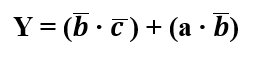
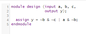
Verilog Code
Verilog Testbench
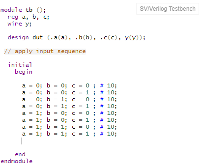
In the Verilog testbench, all the inputs become reg and output a wire. The Testbench simply instantiates the design under test (DUT). It applies a series of inputs. The outputs should be observed and compared by using a simulator program. The initial statement is similar to always; it starts once initially and does not repeat. The statements have to be blocking.
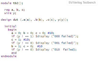
Self-checking Testbench
Self-checking test benches are better than regular Testbenchs; these test benches ensure the design’s functionality on their own. These kinds of Testbench also include a statement to check the current state $display will write a message in the simulator that will help the verification engineer see the design outcomes visually. The Self-Checking test benches effectiveness comes into play when you have a more significant design like a 32-bit processor, and you want to verify the outcome of the instruction, so rather than write a simple test bench, it is wise to use the self-checking Testbench to save time and verification cost.
Verilog Testbench Example – Self Checking
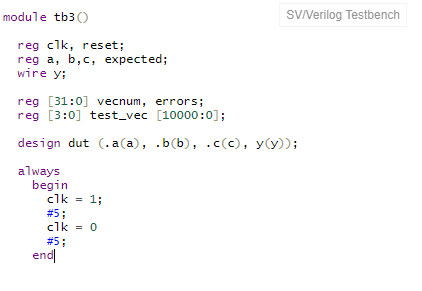
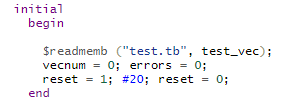
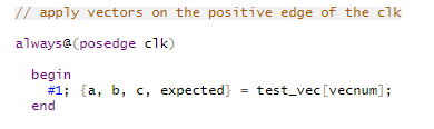
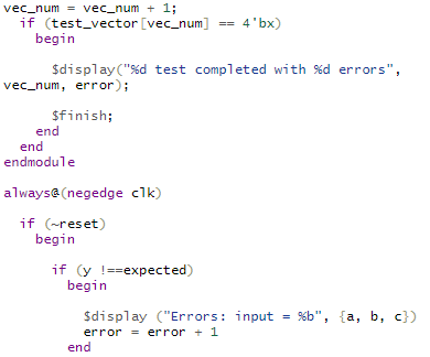
Testbench with Test Vectors
The more elaborated Testbench is to write the test vector file: inputs and expected outputs. Usually, it can use a high-level model name the golden model to produce the “correct” input-output vectors. The process for the Testbench with test vectors are straightforward:
- Generate clock for assigning inputs. A testbench clock is used to synchronize the available input and outputs. The same clock can be used for the DUT clock. So, both design and Testbench have the same frequency.
- Reading Outputs, Read test vectors file and put data into the array.
- Assign inputs, get expected outputs from DUT.
- Compare outputs to expected outputs and report errors.
Verilog Testbench Example – Test Vector
File: example.v – contains vectors of abc_yexpected: 000_1 001_0 010_0 011_0 100_1 101_1 110_0 111_0 (file expected outputs).
Generate Clock
Read Test Vectors into Array
Assign Inputs and Expected Outputs
Compare Outputs with Expected Outputs
Initial / Always Blocks
Always and initial blocks are two main sequential control blocks that operate on reg types in a Verilog simulation. Each initial and always block executes concurrently in every module at the start of the simulation.
The Initial Block Example
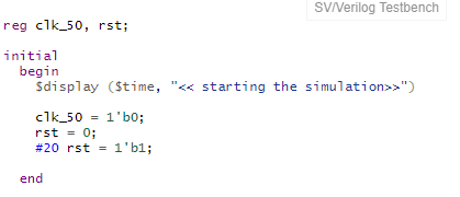
The initial block starts sequentially, displays the simulation’s time, and then sets the clk_50 to 0 and rst_1 to 0. And, after that, release the reset, and set it to 1 after 20 time period.
The always Block Example
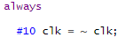
The always block runs every #10 ns starting at time index 0 ns. Therefore, the value of clk_50 will invert from the initialized value. This originates a clock pulse to be generated on clk_50 with a period of 20 ns or a frequency of 50 Mhz.
Delays
At the top of compiler directive: timescale 2 ns / 1000 ps is written.
This line is vital in a Verilog simulation because it sets up the timescale and operational precision for a design. It origins the unit delays to be in nanoseconds (ns) and the accuracy at which the simulator will round the procedures down to 1000 ps. This causes a #2 or #4 in a Verilog assignment to be a 2 ns or 4 ns delay, respectively.
Printing data during Simulations Runs
As a simulation runs, it’s significant to contain printout data to the screen to inform the designer on the position/ status of the existing simulation data. The value a net or register embraces at a particular time in the simulation may be imperative in debugging a function, so signals can also be printed. Two of the most mutual instructions to print to the screen are:
$display
$display is being used to print to a line and enter a carriage return (CRr) at the end. The variables used to display the variables’ format can be: binary using %b, hex using %h, or decimal using %d.
$display(“Hello World!”);
mystring = “This is my string”;
$display(“mystring is %0s”, mystring);
$monitor
$monitor: The monitor precisely monitors the variables or signals in a simulation. Whenever one of the signals/variable changes value, a $monitor can be used to track it down. Only a single $monitor can be active simultaneously in a simulation, but it can prove to be a valued debugging tool.
$monitor (“format_string”, parameter_1, parameter_2, … );
$monitor(“x=%3b,y=%3d,z=%b n”,x,y,z);
Tasks
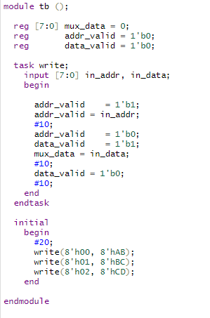
Tasks are used to group a set of repetitive or related commands that would typically be contained in an initial or permanently block. A task can have inputs, outputs, and inputs and can contain timing or delay elements.
This task code takes two eight-bit input vector, and at the positive edge of the next clock signal, it starts executing. It initially depends on the address, data and the mux input. The task block calls into the initial block call for three different inputs and performs the same operations on the different inputs.
Following are some recommendations that apply to all kind of simulation techniques as mentioned above:
- Initialize all the input ports at simulation time zero but do not initiate the expected stimulus for 100 (ns). The purpose is to hold off the input until set/reset has completed.
- The clock must be stable before applying the input data to the input ports.
- Output checking must be synchronized with the clock.
In this post we look at how we use Verilog to write a basic testbench. We start by looking at the architecture of a Verilog testbench before considering some key concepts in verilog testbench design. This includes modelling time in verilog, the initial block, verilog-initial-block and the verilog system tasks. Finally, we go through a complete verilog testbench example.
When using verilog to design digital circuits, we normally also create a testbench to stimulate the code and ensure that it functions as expected.
We can write our testbench using a variety of languages, with VHDL, Verilog and System Verilog being the most popular.
System Verilog is widely adopted in industry and is probably the most common language to use. If you are hoping to design FPGAs professionally, then it will be important to learn this skill at some point.
As it is better to focus on one language as a time, this blog post introduces the basic principles of testbench design in verilog. This allows us to test designs while working through the verilog tutorials on this site.
If you are interested in learning more about testbench design using either verilog or SystemVerilog, then there are several excellent courses paid course available on sites such as udemy.
Architecture of a Basic Testbench
Testbenches consist of non-synthesizable verilog code which generates inputs to the design and checks that the outputs are correct.
The diagram below shows the typical architecture of a simple testbench.

The stimulus block generates the inputs to our FPGA design and the output checker tests the outputs to ensure they have the correct values.
The stimulus and output checker will be in separate files for larger designs. It is also possible to include all of these different elements in a single file.
The main purpose of this post is to introduce the skills which will allow us to test our solutions to the exercises on this site.
Therefore, we don’t discuss the output checking block as it adds unnecessary complexity.
Instead, we can use a simulation tool which allows for waveforms to be viewed directly. The freely available software packages from Xilinx (Vivado) and Intel (Quartus) both offer this capability.
Alternatively, open source tools such as icarus verilog can be used in conjunction with GTKWave to run verilog simulations.
We can also make use of EDA playground which is a free online verilog simulation tool.
In this case, we would need to use system tasks to monitor the outputs of our design. This gives us a textual output which we can use to check the state of our signals at given times in our simulation.
Instantiating the DUT
The first step in writing a testbench is creating a verilog module which acts as the top level of the test.
Unlike the verilog modules we have discussed so far, we want to create a module which has no inputs or outputs in this case. This is because we want the testbench module to be totally self contained.
The code snippet below shows the syntax for an empty module which we can use as our testbench.
module <module_name> ();

 // Our testbench code goes here

endmodule : <module_name>
After we have created a testbench module, we must then instantiate the design which we are testing. This allows us to connect signals to the design in order to stimulate the code.
We have already discussed how we instantiate modules in the previous post on verilog modules. However, the code snippet below shows how this is done using named instantiation.
<module_name> # (
  // If the module uses parameters they are connected here
  .<parameter_name> (<parameter_value>)
)
<instance_name> (
  // Connection to the module ports
  .<port_name> (<signal_name>),
  .<port_name> (signal_name>)
);
Once we have done this, we are ready to start writing our stimulus to the FPGA. This includes generating the clock and reset, as well creating test data to send to the FPGA.
In order to this we need to use some verilog constructs which we have not yet encountered — initial blocks, forever loops and time consuming statements.
We will look at these in more detail before we go through a complete verilog testbench example.
Modelling Time in Verilog
One of the key differences between testbench code and design code is that we don’t need to synthesize the testbench.
As a result of this, we can use special constructs which consume time. In fact, this is crucial for creating test stimulus.
We have a construct available to us in Verilog which enables us to model delays. In verilog, we use the # character followed by a number of time units to model delays.
As an example, the verilog code below shows an example of using the delay operator to wait for 10 time units.
One important thing to note here is that there is no semi-colon at the end of the code. When we write code to model a delay in Verilog, this would actually result in compilation errors.
It is also common to write the delay in the same line of code as the assignment. This effectively acts as a scheduler, meaning that the change in signal is scheduled to take place after the delay time.
The code snippet below shows an example of this type of code.
// A is set to 1 after 10 time units
#10 a = 1'b1;
Timescale Compiler Directive
So far, we have talked about delays which are ten units of time. This is fairly meaningless until we actually define what time units we should use.
In order to specify the time units that we use during simulation, we use a verilog compiler directive which specifies the time unit and resolution. We only need to do this once in our testbench and it should be done outside of a module.
The code snippet below shows the compiler directive we use to specify the time units in verilog.
`timescale <unit_time> / <resolution>
We use the <unit_time> field to specify the main time unit of our testbench and the <resolution> field to define the resolution of the time units in our simulation.
The <resolution> field is important as we can use non-integer numbers to specify the delay in our verilog code. For example, if we want to have a delay of 10.5ns, we could simply write #10.5 as the delay.
Therefore, the <resolution> field in the compiler directive determines the smallest time step we can actually model in our Verilog code.
Both of the fields in this compiler directive take a time type such as 1ps or 1ns.
Verilog initial block
In the post on always blocks in verilog, we saw how we can use procedural blocks to execute code sequentially.
Another type of procedural block which we can use in verilog is known as the initial block.
Any code which we write inside an initial block is executed once, and only once, at the beginning of a simulation.
The verilog code below shows the syntax we use for an initial block.
initial begin
  // Our code goes here
end
Unlike the always block, verilog code written within initial block is not synthesizable. As a result of this, we use them almost exclusively for simulation purposes.
However, we can also use initial blocks in our verilog RTL to initialise signals.
When we write stimulus code in our verilog testbench we almost always use the initial block.
To give a better understanding of how we use the initial block to write stimulus in verilog, let’s consider a basic example.
For this example imagine that we want to test a basic two input and gate.
To do this, we would need code which generates each of the four possible input combinations.
In addition, we would also need to use the delay operator in order to wait for some time between generating the inputs.
This is important as it allows time for the signals to propagate through our design.
The verilog code below shows the method we would use to write this test within an initial block.
initial begin
  // Generate each input to an AND gate
  // Waiting 10 time units between each
  and_in = 2b'00;
  #10
  and_in = 2b'01;
  #10
  and_in = 2b'10;
  #10
  and_in = 2b'11;
 end
Verilog forever loop
Although we haven’t yet discussed loops, they can be used to perform important functions in Verilog. In fact, we will discuss verilog loops in detail in a later post in this series
However, there is one important type of loop which we can use in a verilog testbench — the forever loop.
When we use this construct we are actually creating an infinite loop. This means we create a section of code which runs contimnuously during our simulation.
The verilog code below shows the syntax we use to write forever loops.
forever begin
  // our code goes here
end
When writing code in other programming languages, we would likely consider an infinite loop as a serious bug which should be avoided.
However, we must remember that verilog is not like other programming languages. When we write verilog code we are describing hardware and not writing software.
Therefore, we have at least one case where we can use an infinite loop — to generate a clock signal in our verilog testbench.
To do this, we need a way of continually inverting the signal at regular intervals. The forever loop provides us with an easy method to implement this.
The verilog code below shows how we can use the forever loop to generate a clock in our testbench. It is important to note that any loops we write must be contained with in a procedural block or generate block.
 initial begin
    clk = 1'b0;
    forever begin
      #1 clk = ~clk;
    end
  end
Verilog System Tasks
When we write testbenches in verilog, we have some inbuilt tasks and functions which we can use to help us.
Collectively, these are known as system tasks or system functions and we can identify them easily as they always begin wtih a dollar symbol.
There are actually several of these tasks available. However, we will only look at three of the most commonly used verilog system tasks — $display, $monitor and $time.
$display
The $display function is one of the most commonly used system tasks in verilog. We use this to output a message which is displayed on the console during simulation.
We use the $display macro in a very similar way to the printf function in C.
This means we can easily create text statements in our testbench and use them to display information about the status of our simulation.
We can also use a special character (%) in the string to display signals in our design. When we do this we must also include a format letter which tells the task what format to display the variable in.
The most commonly used format codes are b (binary), d (decimal) and h (hex). We can also include a number in front of this format code to determine the number of digits to display.
The verilog code below shows the general syntax for the $display system task. This code snippet also includes an example use case.
// General syntax
$display(<string_to_display>, <variables_to_display);

// Example - display value of x as a binary, hex and decimal number
$display("x (bin) = %b, x (hex) = %h, x (decimal) = %d", x, x, x);
The full list of different formats we can use with the $display system task are shown in the table below.
| Format Code | Description |
|---|---|
| %b or %B | Display as binary |
| %d or %D | Display as decimal |
| %h or %H | Display as hexidecimal |
| %o or %O | Display as octal format |
| %c or %C | Display as ASCII character |
| %m or %M | Display the hierarchical name of our module |
| %s or %S | Display as a string |
| %t or %T | Display as time |
$monitor
The $monitor function is very similar to the $display function, except that it has slightly more intelligent behaviour.
We use this function to monitor the value of signals in our testbench and display a message whenever one of these signals changes state.
All system tasks are actually ignored by the synthesizer so we could even include $monitor statements in our verilog RTL code, although this is not common.
The general syntax for this system task is shown in the code snippet below. This code snippet also includes an example use case.
// General syntax
$monitor(<message_to_display>, <variables_to_display>);

// Example - monitor the values of the in_a and in_b signals
$monitor("in_a=%b, in_b=%bn", in_a, in_b);
$time
The final system task which we commonly use in testbenches is the $time function. We use this system task to get the current simulation time.
In our verilog testbenches, we commonly use the $time function together with either the $display or $monitor tasks to display the time in our messages.
The verilog code below shows how we use the $time and $display tasks together to create a message.
$display("Current simulation time = %t", $time);
Verilog Testbench Example
Now that we have discussed the most important topics for testbench design, let’s consider a compete example.
We will use a very simple circuit for this and build a testbench which generates every possible input combination.
The circuit shown below is the one we will use for this example. This consists of a simple two input and gate as well as a flip flip.

1. Create a Testbench Module
The first thing we do in the testbench is declare an empty module to write our testbench code in.
The code snippet below shows the declaration of the module for this testbench.
Note that it is good practise to keep the name of the design being tested and the testbench similar. Normally this is done by simply appending _tb or _test to the end of the design name.
module example_tb ();

  // Our testbench code goes here

endmodule : example_tb
2. Instantiate the DUT
Now that we have a blank testbench module to work with, we need to instantiate the design we are going to test.
As named instantiation is generally easy to maintain than positional instantiation, as well as being easier to understand, this is the method we use.
The code snippet below shows how we would instantiate the DUT, assuming that the signals clk, in_1, in_b and out_q are declared previously.
example_design dut (
    .clock (clk),
    .reset (reset),
    .a     (in_a),
    .b     (in_b),
    .q     (out_q)
  );
3. Generate the Clock and Reset
The next thing we do is generate a clock and reset signal in our verilog testbench.
In both cases, we can write the code for this within an initial block. We then use the verilog delay operator to schedule the changes of state.
In the case of the clock signal, we use the forever keyword to continually run the clock signal during our tests.
Using this construct, we schedule an inversion every 1 ns, giving a clock frequency of 500MHz.
This frequency is chosen purely to give a fast simulation time. In reality, 500MHz clock rates in FPGAs are difficult to achieve and the testbench clock frequency should match the frequency of the hardware clock.
The verilog code below shows how the clock and the reset signals are generated in our testbench.
// generate the clock
  initial begin
    clk = 1'b0;
    forever #1 clk = ~clk;
  end

  // Generate the reset
  initial begin
   reset = 1'b1;
    #10
   reset = 1'b0;
  end
4. Write the Stimulus
The final part of the testbench that we need to write is the test stimulus.
In order to test the circuit we need to generate each of the four possible input combinations in turn. We then need to wait for a short time while the signals propagate through our code block.
To do this, we assign the inputs a value and then use the verilog delay operator to allow for propagation through the FPGA.
We also want to monitor the values of the inputs and outputs, which we can do with the $monitor verilog system task.
The code snippet below shows the code for this.
initial begin
    // Use the monitor task to display the FPGA IO
    $monitor("time=%3d, in_a=%b, in_b=%b, q=%2b n",
              $time, in_a, in_b, q);

    // Generate each input with a 20 ns delay between them
    in_a = 1'b0;
    in_b = 1'b0;
    #20
    in_a = 1'b1;
    #20
    in_a = 1'b0;
    in_b = 1'b1;
    #20
    in_a = 1'b1;
  end
Full Example Code
The verilog code below shows the testbench example in its entirety.
`timescale 1ns / 1ps

module example_tb ();
  // Clock and reset signals
  reg clk;
  reg reset;

  // Design Inputs and outputs
  reg in_a;
  reg in_b;
  wire out_q;

  // DUT instantiation
  example_design dut (
    .clock (clk),
    .reset (reset),
    .a     (in_a),
    .b     (in_b),
    .q     (out_q)
  );

  // generate the clock
  initial begin
    clk = 1'b0;
    forever #1 clk = ~clk;
  end

  // Generate the reset
  initial begin
   reset = 1'b1;
    #10
   reset = 1'b0;
  end

  // Test stimulus
  initial begin
    // Use the monitor task to display the FPGA IO
    $monitor("time=%3d, in_a=%b, in_b=%b, q=%2b n",
              $time, in_a, in_b, q);

    // Generate each input with a 20 ns delay between them
    in_a = 1'b0;
    in_b = 1'b0;
    #20
    in_a = 1'b1;
    #20
    in_a = 1'b0;
    in_b = 1'b1;
    #20
    in_a = 1'b1;
  end

endmodule : example_tb
Exercises
When using a basic testbench architecture which block generates inputs to the DUT?
show answer
The stimulus block is used to generate inputs to the DUT.
hide answer
Write an empty verilog module which can be used as a verilog testbench.
show answer
module example_tb ();

  // Our test bench code goes here

endmodule : example_tb
hide answer
Why is named instantiation generally preferable to positional instantiation.
show answer
It is easier to maintain our code as the module connections are explicitly given.
hide answer
What is the difference between the $display and $monitor verilog system tasks.
show answer
The $display task runs once whenever it is called. The $monitor task monitors a number of signals and displays a message whenever one of them changes state,
hide answer
Write some verilog code which generates stimulus for a 3 input AND gate with a delay of 10 ns each time the inputs change state.
show answer
`timescale 1ns / 1ps

intial begin
  and_in = 3'b000;
  #10
  and_in = 3'b001;
  #10
  and_in = 3'b010;
  #10
  and_in = 3'b011;
  #10
  and_in = 3'b100;
  #10
  and_in = 3'b101;
  #10
  and_in = 3'b110;
  #10
end
hide answer
The testbench is written to check the functional correctness based on design behavior. The connections between design and testbench are established using a port interface. A testbench generates and drives a stimulus to the design to check its behavior. Since the behavior of the design has to be tested, the design module is known to be “Design Under Test” (DUT).
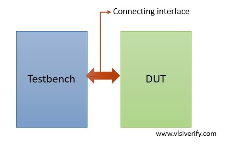
Connection between testbench and DUT
Let’s understand how to write Verilog testbench with a simple example of 2:1 MUX.
A 2:1 MUX is implemented using the ‘assign statement’ which will be discussed in the dataflow modeling section. For now, it is better to focus on how DUT is connected with a testbench and how the generated stimulus is driven.
module mux_2_1(
  input sel,
  input i0, i1,
  output y);

  assign y = sel ? i1 : i0;
endmodule
Steps involved in writing a Verilog testbench
i. Declare a testbench as a module.
module <testbench_name>;
Example: module mux_tb;
ii. Declare set signals that have to be driven to the DUT. The signals which are connected to the input of the design can be termed as ‘driving signals’ whereas the signals which are connected to the output of the design can be termed as ‘monitoring signals’. The driving signal should be of reg type because it can hold a value and it is mainly assigned in a procedural block (initial and always blocks). The monitoring signals should be of net (wire) type that get value driven by the DUT.
Note: The testbench signal nomenclature can be different the DUT port
reg i0, i1, sel; // declaration.
wire y;
iii. Instantiate top-level design and connect DUT port interface with testbench variables or signals.
<dut_module> <dut_inst> (<TB signals>)
mux_2_1 mux(.sel(sel), .i0(i0), .i1(i1), .y(y));
or
mux_2_1 mux(sel, i0, i1, y);
iv. Use an initial block to set variable values and it can be changed after some delay based on the requirement. The initial block execution starts at the beginning of the simulation and updated values will be propagated to an input port of the DUT. The initial block is also used to initialize the variables in order to avoid x propagation to the DUT.
Example: Initialize clock and reset variables.
initial begin
  clock = 0;
  reset = 0;
end
initial begin
// To print the values.
$monitor("sel = %h: i0 = %h, i1 = %h --> y = %h", sel, i0, i1, y);
i0 = 0; i1 = 1;
sel = 0;
#1;
sel = 1;
endv. An always block can also be used to perform certain actions throughout the simulation.
Example: Toggling a clock
always #2 clock = ~ clock;In the above example, the clock is not used in the DUT, so we will not be declaring or using it.
vi. The system task $finish is used to terminate the simulation based on the requirement.
vii. The endmodule keyword is used to complete the testbench structure.
Complete testbench code
module mux_tb;
  reg i0, i1, sel;
  wire y;

  mux_2_1 mux(sel, i0, i1, y);
  initial begin
    $monitor("sel = %h: i0 = %h, i1 = %h --> y = %h", sel, i0, i1, y);
    i0 = 0; i1 = 1;
    sel = 0;
    #1;
    sel = 1;
  end
endmoduleHow to start a new Vivado project to create a testbench for programming with Verilog or VHDL languages.
It is very common with the students, who are trying to learn a new programming language, to only read and understand the codes on the books or online.
But until you don’t put hands-on and start typing your own small programs, compile them, find errors, simulate, etc you will not get the experience to write your own codes and therefore to learn how to program a new language.

In this small tutorial, I am going to explain step by step how to create your testbench in Vivado, so you can start a Vivado Project, begin to program and boost your Verilog or VHDL learning.
Download Vivado
If you don’t have it, download the free Vivado version from the Xilinx web. For that you will need to register in Xilinx and then get the “Vivado HLx 20XX: WebPACK and Editions Self Extracting Web Installer”.
The download-file is not so big, because during the installation it will download the necessary files. It will take a lot of time, around 1 or 2 hours.
Then open Vivado:
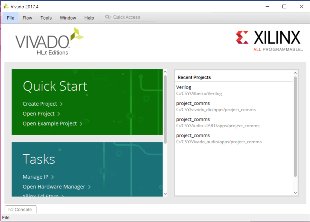
New Vivado Project
Create a new project with the assistant with File>>New Project…

Give a name and a project directory to store all the related files. In this example, I chose C:// as project location.

The type of the project should be an RTL project. If you start an empty project, you don’t have any source to add to the project, therefore check the box “Do not specify at this time”.
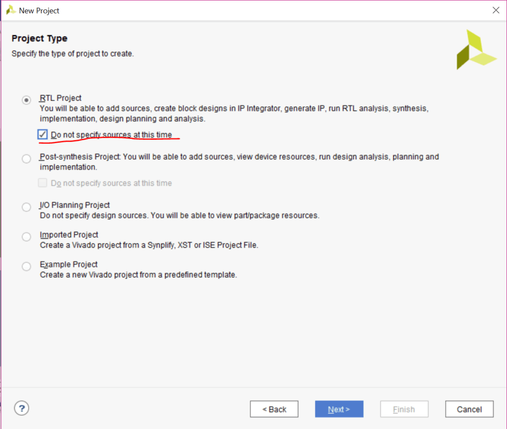
As we want to only simulate, we are not going to select any hardware. If desired this can be chosen later.

Click “Finish” and the new project will be opened.

Vivado Dashboard
The Vivado dashboard is now opened. You will get familiar with each window, when you spend some time in Vivado. For small laptop screens (as mine), it is a bit awkward to show all the information and work comfortably. You will want to maximize temporally the windows, especially the block diagram.
The fast way is to double click on the top bar of each window to maximize it (where the red crosses are) also the maximize button works identically. But I would suggest connecting a second screen to work more efficiently.

Start by creating a new block diagram to be the top of the testbench. On this diagram, all your modules are going to be placed and tested.
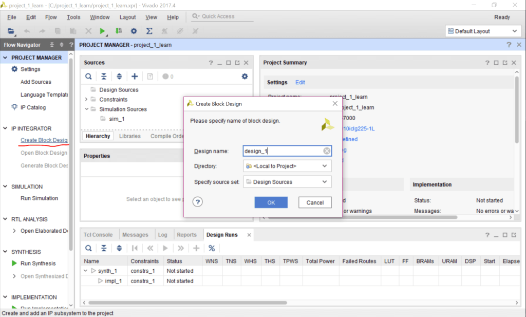
The new block diagram is now created:
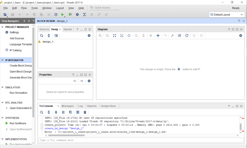
Click on “Add sources” to create the modules:

Click on “Create File”:

Give a name to the RTL module, select Verilog as file type and then press OK and then Finish. 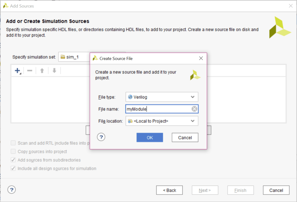
Vivado will ask you to configure the inputs and outputs. But this can be done later by code (faster and easier), so for now we skip this step pressing OK.

And when a new window is prompted, press Yes, we are sure!

Now, we are going to add some code in the module. By double click on the sources, a window will open.

There you can start typing your code. The automatic template for an RTL module in Vivado has a very big header. I hate it. You can remove it or leave it smaller as I did.

In this example I wrote a simply asynchronous and-gate in Verilog:

`timescale 1ns / 1ps
module myModule(A, B, result);
    input A;
    input B;
    output result;

    assign result A & B;

endmodule
For the simulation, a stimuli block or wave generator will be needed to stimulate your modules under test, in this example the and-gate. For this a new module named “Stimuli” as before is created.
`timescale 1ns / 1ps
module FlipFlop( D, clk, Q);
    input D;
    input clk;
    output Q;

    reg r_FF;

    always @ (posedge clk)
    begin
        r_FF <= D;
    end

    assign Q = r_FF;

endmodule
The following example of Stimuli can be copied as a reference:
`timescale 1ns / 1ps
module Stimuli( A, B, clk);
output A;
output B;
output reg clk;

always
    begin
        clk = 1’b1;
        #5;
        clk = 1’b0;
        #5; // 10ns period
    end

initial begin
    begin
        A =  $urandom_range(0,1); //random value between 0 and 1
        B = 1’b0;
        #10 //wait 10 nanosecons
        B = 1’b1;
        #30
        A = 1’b0;
        B = $urandom_range(0,1);
        //to be continued...
    end
endmodule
The created modules should be added to the block diagram to interconnect them. For that right-click on the diagram and then select “Add Module…”

Both modules can be added.

And then, we can connect the blocks with each other, just wiring the signals.

To be able to simulate, Vivado needs a Wrapper over the block diagram. This wrapper is a file that connects the output/input port of your block diagram to the physical pin described in the constraint file. In this case, we don’t have yet a constrain file, but Vivado requests it.
For that we create an HDL Wrapper by right click on the block diagram sources:

Then we choose “Let Vivado manage the wrapper…”

After the wrapper is created, we to need to say to Vivado which file is our top level. This is made in Simulation settings… Right-click on the word “SIMULATION”.

The setting should be checked and changed.

Now everything should be ready for our first simulation! We click on the left panel on “Run simulation” and the simulation view will open.

The signal to be plotted should be dragged into the wave diagram to see them. After that, we can click on run for a finite among of time, in this case, 120 ns. To fit the time-scale you can press the on the symbol ![]() .
.

These are the basic steps to start a simulation of your own RTL modules in Vivado. Now you should be able to simulate Verilog modules to compile and test them.
Vivado is complex, so be patient and persistent!
Все статьи цикла
Что такое «testbench»?
Этим термином обычно обозначают код для проверки проекта пользователя при симуляции. Код создан для того, чтобы описать, какие действия будут осуществлены с проверяемым модулем, и увидеть его ответную реакцию.
Как было сказано в предыдущих разделах, процесс проектирования начинается с того, что уточняется задание на проект и вырабатываются проектные спецификации. Далее идет разработка файлов проекта. И одновременно с этим начинается верификация, то есть проверка проекта. Весь процесс верификации сводится к тому, что разработчик сравнивает то, что он должен получить от изделия, с тем, что он наблюдает в поведении проверяемого проекта (рис. 1). На основании сравнения разработчик определяет, соответствует ли ожидаемое поведение проекта полученному.

Рис. 1. Сравнение поведения проверяемого проекта с тем, что должно получиться по заданию на проектирование
Всякий раз, когда описывается концепция тестирования или описывается методика работы тестбенча, необходимо ясно отличать опорный проект и тестируемый проект (DUT design under test).
DUT представляет собой проект в некоторой законченной форме, подходящей для воплощения в продукции. Опорный проект это идеальный вариант, «мечта» проектировщика, или то, что должен выполнять данный проект в соответствии с техническим заданием. Компонент для сравнения может быть выполнен во множестве форм, например, это может быть документ, описывающий работу DUT, некоторая опорная модель, которая содержит уникальный алгоритм, или это могут быть различные протоколы обмена данных.
Создание проекта это отдельная проблема, и она должна быть хорошо понятна разработчикам. В этом разделе мы ограничимся обсуждением проблем по фиксации того, что данный проект создан в соответствии с выданными техническими требованиями.
Два основных вопроса
Завершением любого проекта можно считать тот момент, кода будут получены положительные ответы на два основных вопроса: «Это уже работает?» и «Мы это уже сделали?» Это довольно очевидные вопросы, но они основа для любой методики по проверке проекта. Ответ на первый вопрос появляется в соответствии с теми идеями относительно проверки проекта, которые мы обсуждали в предыдущем разделе. Положительный ответ соответствует тому, что выполненный нами проект соответствует выданному заданию на проектируемое изделие. Положительный ответ на второй вопрос означает, что мы сравнили результаты проверки с заданием и пришли к выводу, что разработанный нами проект полностью соответствует заданию, или, в противном случае, почему он ему не соответствует. На рис. 2 показана блоксхема, отражающая обобщенную методику проверки проекта. На данной диаграмме кружочки с цифрами представляют собой основные пункты, по которым должно проходить тестирование проекта.

Рис. 2. Обобщенная блоксхема проведения верификации проекта
Каждый проект проверки начинается со спецификации проекта (п. 1 на диаграмме). Спецификация содержит все детали относительно того, как именно должен быть выполнен данный проект. В мировой практике принято, чтобы проект вели две независимых группы разработчиков: одна группа занимается собственно разработкой функциональных узлов проекта, а другая проверкой проектов. Однако в небольших фирмах разработкой проектов и проверкой занимаются одни и те же люди, но, в ряде случаев, это может привести к росту числа ошибок.
Итак, группа проверки использует спецификацию проекта, чтобы построить план проверки. Это список всех вопросов, на которые нужно ответить в процессе проверки, и описание того, каким способом будут выдаваться ответы. Таким образом, на данном этапе создается контрольный список всех вопросов, на которые необходимо ответить, этот же список вопросов ложится в основу для спецификаций по тестбенчу (п. 2 на диаграмме). В качестве примера можно привести часть стандартного списка вопросов для проверки соответствия разрабатываемого устройства на стандарт шины PCI. Данный список вопросов разработан комитетом по стандарту PCI. В таблице приведены только 3 вопроса из 52. Полный список вопросов можно посмотреть в документах комитета, а также, например, в [2].
| № вопроса | Описание вопроса | Да | Нет |
|---|---|---|---|
| CE45 | Все трехстабильные сигналы переходят в третье состояние не позже чем за 28 нс для шины, работающей на частоте 33 Мгц, и не позднее, чем за 14 нс для шины, работающей на частоте 66 Мгц? |
+ | |
| CE46 | Все входные сигналы на шинах требуют время предустановки не менее чем 7 нс для шины, работающей на частоте 33 Мгц, и не менее чем 3 нс для шины, работающей на частоте 66 Мгц? |
+ | |
| CE47 | Сигнал REQ# требует время предустановки не менее чем 12 нс для шины, работающей на частоте 33 Мгц, и не менее чем 5 нс для шины, работающей на частоте 66 Мгц? | + |
После того, как тестбенч будет создан, начинается этап моделирования проекта совместно с тестбенчем. Результаты моделирования и дадут нам ту информацию, на основании которой мы можем ответить на два заданных вопроса. Первый вопрос «Это уже работает?» Если ответ «Нет», то проект должен быть заново отлажен (что соответствует п. 3 на диаграмме). Отрицательный ответ на вопрос также приводит к тому, что проект должен быть доработан, для того чтобы исправить все выявленные ошибки, недостатки или неточности, которые удалось найти при тестировании.
Когда нам кажется, что проект функционирует должным образом, значит, тогда пришло время задавать следующий вопрос: «Мы это уже сделали?» На диаграмме этому состоянию соответствует п. 4. Сначала необходимо определить, какая часть проекта была охвачена тестированием. Если охват тестированием недостаточен, то объем работ по симуляции и тестбенч должны быть увеличены. Этому состоянию соответствует п. 5.
Конечно, при идеальных условиях проект не будет иметь какихлибо ошибок, и, таким образом, охват тестированием в этом случае всегда будет достаточен. Необходимо пройти только один цикл проверки, чтобы сразу получить положительные ответы на оба вопроса. В реальности же может потребоваться довольно много итераций. Правильная методология проверки проекта как раз и позволяет значительно уменьшить число итераций, чтобы закончить выполнение проверки проекта в кратчайшее время и использовать наименьшее количество ресурсов.
Чтобы читателю были более понятны эти, кажущиеся очевидными, рассуждения, давайте рассмотрим небольшой пример из практики.
Итак, несколько слов о том, как надо и как не надо отлаживать проекты
Представим себе «классический пример». Допустим, у нас есть проект пользователя, представляющий собой UART. UART имеет следующие характеристики: данные на прием и на передачу 8 разрядов, бит проверки на четность и стоповый бит. Частота приема и передачи фиксированная. Тактовая частота системная, сброс системный асинхронный. Пример этот довольно часто встречается при разработке проектов в FPGA. Вроде бы ничего сложного, обычный проект, достойный студента 3го или 4го курса… А теперь давайте составим план проверки проекта.
Первый вариант облегченный
Этим вариантом заканчивают свою работу студенты и так же поступают оптимисты, которые свято верят в то, что проект обязан заработать сам по себе. Причем они с большим удивлением отвечают на вопрос: «А как именно вы проводили проверку проекта?» Они всегда очень уверенно добавляют: «При симуляции у меня проект идеально работал, без сбоев!»
Итак, вот их методика проверки.
Шаг № 1. Делаем файл testbench с UART’ом. Создаем тактовую частоту из системной, путем деления системной частоты на счетчике. Делаем заглушку «передача на прием».
Шаг № 2. Передаем байт данных, принимаем этот же байт, визуально сравниваем переданный и принятый байты. Если они совпали, то на этом проверка завершается.
А как это положено делать?
Для этого надо тщательно проследить, как именно работает наше устройство, и выбрать «крайние» режимы работы.
Шаг № 1. Для начала введем в testbench две системных тактовых частоты: одну для приема, а другую для передачи. Соответственно сделаем и две бодовых частоты: одну для передатчика, другую для приемника. Теперь сформируем массив данных для передачи в виде файла. В testbench сделаем выдачу данных в передатчик из файла, а в приемнике сделаем запись данных в файл принимаемых данных. Дополнительно можно и в testbench сформировать функцию проверки переданных и принятых данных.
Шаг № 2. Делаем системные тактовые частоты равными. Проводим проверку тракта передача/прием. Результат сравниваем в файлах. Если совпали, переходим к следующему шагу.
Шаги № 3 и 4. Моделируем разбег частот генераторов системной тактовой частоты. Генератор «перекашиваем» в разные стороны. Уход частоты генератора статический, временной и температурный. Здесь также необходимо учесть то, что делитель бодовой частоты тоже может давать неточное приближение к стандартной бодовой частоте.
Шаги № 5 и 6. В этом разделе мы будем проверять, формирует ли приемник бит ошибки по паритету. Выполняем проверку, аналогичную пунктам 3 и 4, но на стороне передачи делаем ошибку по паритету. Эту ошибку приемник должен показать в регистре состояний.
Шаги № 7 и 8. Теперь проверим тем же образом стоповый бит. На стороне передачи создаем неправильную посылку по стоповому биту. Эту ошибку приемник тоже должен показать в регистре состояний.
Шаг № 9. Мы проверили работу передатчика и приемника при идеальной линии связи. Теперь необходимо проверить работу приемника при сбойных импульсах в линии. Формируем «короткий» стартовый импульс в линии. Выберем одно из «крайних» значений тактового генератора и проводим тест. Приемник не должен принимать данные, но в регистре состояний может появиться соответствующий бит.
Шаг № 10. Осталось самое легкое: введем сбойные биты «внутрь» битового интервала данных на передаче. Если в приемнике сделан мажоритар, то он должен восстановить правильное значение данных.
Итак, 10 шагов, вместо 2 шагов в предыдущем случае. Какой из этого можно сделать вывод? Еще раз обратимся к классику (см. [3] во 2й части данной статьи). Вот что пишет Жаник Бергерон: «До 70% трудозатрат в проекте приходится на верификацию проекта».
Несколько слов об «отладке проекта» до «отладки проекта»
Прежде чем переходить к описаниям тестбенчей и к примерам их реализации, необходимо сказать несколько слов о том, что под термином «отладка проекта» необходимо понимать не только обычную отладку при помощи программ симуляторов аппаратных средств, но можно и должно понимать отладку проекта при помощи обычных программных средств, таких как Си или MathCAD.
Вот пример из реальной практики. Автору необходимо было отладить многоканальный HDLCконтроллер. Проект представлял собой специализированный вычислитель, который на каждом из 32 таймслотов перезагружался, производил свои вычисления для одного байта данных из текущего таймслота и результаты вычислений сбрасывал в память. Для того чтобы отладить такой проект, необходимо было либо выполнить его по частям, то есть сделать только одноканальный контроллер, пропустить через него достаточно большой пакет данных и убедиться, что проект работает верно. А затем дополнить данный проект до полного 32канального варианта. И тогда представим себе диаграмму: 32 канала таймслота, во время каждого таймслота вычислитель делает 1020 действий по одному такту. Всего получим до 600 тактов. Теперь представим, что мы хотим промоделировать прием последовательности из 20 байт. Следовательно, получим до 1200 тактов. Что тут можно сказать? Процесс долгий, кропотливый и неблагодарный. Автор в этом случае избрал совершенно другой путь. К разработке был привлечен программист: ему впоследствии надо было писать программы для прибора, в который входил и этот контроллер. Следовательно, для проверки прибора все равно необходимо было сделать конвертер данных, который бы из входной HDLCпоследовательности мог бы извлекать кадры данных. Такая программная модель контроллера и была сделана. Именно на ней были опробованы все алгоритмы работы контроллера. Причем при создании этой модели разработчики старались написать код программы на Си так, чтобы он был более всего похож на «железо». Потом осталось только заменить переменные языка Си на регистры и триггеры в FPGA.
И еще одно замечание о пользе программных инструментов. Применение программных инструментов позволяет значительно сократить число ошибок при разработке. В качестве примеров автор может привести свои статьи [2] (см. также [1] в 6й части данной статьи), в которых описаны программные инструменты, примененные им в своих разработках. И конечно, не надо забывать, что существует достаточно много документов, в которых описано применение различных программ, позволяющих ускорить проектирование (см. [3] в 6й части данной статьи). В любом случае полезно проверить наличие такой документации на сайтах фирмпроизводителей и фирм, разработчиков программных инструментов, даже если вы не планируете работать с продукцией данной фирмы.
Тестбенч (испытательный стенд)
В этом разделе мы уже ввели термин тестбенч, который здесь можно рассматривать как испытательный стенд. В наиболее общей канонической форме тестбенч сравнивает результаты, полученные при симуляции работы DUT, с ожидаемыми результатами (рис. 3). Благодаря такому тестбенчу можно дать ответ на вопрос: «Это уже работает?» Если фактические результаты соответствуют ожидаемым результатам, то проверяемое устройство действительно работает, по крайней мере, с той точки зрения, что полученный набор ожидаемых результатов соответствует требуемым.

Рис. 3. Обобщенная модель тестбенча
Базовый тестбенч имеет: файл стимуляционных воздействий на DUT, средство для того, чтобы применить стимуляционные воздействия к проекту, и средства для того, чтобы собрать полученные от DUT результаты. После проведения тестирования и получения образцовых результатов их можно будет сравнить с ожидаемыми результатами, полученными от работы проверяемого проекта. Поскольку простой проект с небольшим количеством входов имеет обычно и немного состояний, то набор ожидаемых результатов может быть просто построен вручную. Для любого проекта даже умеренной сложности подобная задача может быть достаточно трудоемкой. В таком случае более продуктивный способ состоит в том, чтобы создать образцовую модель, которая будет генерировать ожидаемые результаты. На рис. 4 показана структура тестбенча, где ожидаемые результаты и результаты, полученные от DUT, будут сгенерированы из того же самого набора стимулирующих воздействий. Если DUT будет работать правильно, то компаратор покажет, что работа, выполненная образцовой моделью и DUT, идентична.

Рис. 4. Основной вариант тестбенча с опорной моделью
Точно так же как и в варианте с образцовой моделью, есть еще одна возможность не выполнять непосредственно набор стимулирующих воздействий как некоторую последовательность векторов. Обычно гораздо проще написать программу, которая и будет генерировать стимулирующие воздействия. Поэтому, возможно, не будет необходимости хранить в файле набор стимулирующих воздействий или результаты работы теста. Вместо этого генератор стимулирующих воздействий сможет генерировать набор таких воздействий непосредственно в темпе выполнения тестирования, и компаратор может сравнить результаты работы по мере того, как они вырабатываются. Это обеспечивает более автоматизированный процесс, где процесс выработки набора стимулирующих воздействий и процесс сравнения результатов будет выполнен как часть тестбенча (рис. 5).

Рис 5. Автоматизированный тестбенч
Теперь давайте поднимемся еще на одну ступень выше. Если мы заменим блок под названием «компаратор» на другой блок, который можно образно назвать так: блок, «отвечающий за то, что проверка выполнена», то в этом случае мы сможем обрабатывать более сложные наборы данных. И этот новый блок будет отвечать на ряд вопросов, среди которых наиболее важным будет следующий: «Действительно ли функционирование DUT соответствует функционированию опорной модели?» Таким образом, новый блок позволит более эффективно производить проверку проекта по сравнению с предыдущим случаем, когда мы лишь сравнивали фактически полученные результаты с ожидаемыми. И такой блок мы будем называть «блоком результатов тестирования» (scoreboard).
При проверке блок результатов тестирования получает информацию от референсных компонентов, которые выдают образцовые значения данных, сгенерированных в течение моделирования при проверке DUT. Вся информация, которая при этом собирается, должна помочь выработать решение о проверке. Другой вопрос, на который также необходимо получить ответ: «Мы это уже сделали?» Для того чтобы принять это решение, мы можем использовать информацию, которая будет собрана в блоке коллекторе охвата (coverage collector). Он получает информацию от генераторов стимулирующих воздействий, из блока результатов тестирования, и от DUT обо всем том, что произошло в течение моделирования. Вариант такого тестбенча с блоком результатов тестирования и коллектором охвата показан на рис. 6.

Рис. 6. Обобщенный вариант тестбенча
Выводы:
- Генераторы стимулирующих воздействий инициализируют тестирование проекта. Те же самые стимулирующие воздействия посылаются как проекту при тесте, так и блоку принятия решений и/или опорной модели.
- Блок результатов тестирования оценивает поведение DUT и отвечает на вопрос «Это уже работает?» Блок результатов тестирования может включать в себя опорную модель.
- Коллектор охвата собирает информацию о работе DUT во время моделирования. Информацию в коллекторе охвата можно использовать для того, чтобы ответить на вопрос: «Мы это уже сделали?»
О стиле написания тестбенча
Здесь необходимо привести один пример (см. [3] из 2й части данной статьи). Представим, что нам надо написать небольшой тестбенч для проверки некоторого узла. Как это будет выглядеть? Есть две точки зрения на этот вопрос. Разделим инженеров на две группы в соответствии с их навыками в написании тестбенчей. Первая группа это опытные инженерыразработчики, вторая инженерытестировщики.
Инженерыразработчики легко справляются с заданиями, в которых нужно выполнять синтезируемые модели. Такие модели содержат набор VHDL или Verilogфайлов, и в них соблюдается один или только несколько стилей RTLпрограммирования. Есть довольно много публикаций по стилям RTL-программирования с рекомендациями по оптимизации проекта по занимаемой площади, скорости или потребляемой мощности.
Здесь еще раз приведены основные правила кодирования, которые помогают избежать нежелательных аппаратных компонентов, таких как триггерызащелки, лишние внутренние шины или трехстабильные буферы.
Вот эти правила RTLкодирования:
- Чтобы избежать триггеровзащелок, необходимо устанавливать в начале блока все выходы комбинаторных блоков в состояние по умолчанию.
- Чтобы избежать внутренних шин, не выполняйте назначения регистрам (assign reg) из двух различных блоков always.
- Чтобы избежать трехстабильных буферов, не присваивайте значения Z (например, 1’bz).
Дополним эти правила:
- Все входы блока, состоящего только из комбинационной логики, должны быть перечислены в списке чувствительности.
- Синхрочастота и асинхронный сброс должны быть в списке чувствительности блока, содержащего последовательные компоненты триггеры и регистры.
- Используйте неблокирующие назначения для переменных типа reg, которые в проекте будут установлены как триггеры или регистры.
Инженерыаппаратчики мыслят категориями статических автоматов, мультиплексоров, декодеров, триггеровзащелок, тактовых частот и т. д. Но не используйте стиль RTLкодирования, когда вы пишете тестбенчи. Для того чтобы сделать конечный проект, который будет загружаться в изделие, у HDLязыков мало «выразительных средств». Эти средства определяются применяемой технологией и аппаратной платформой. А в том случае, когда нужно написать тестбенч, никаких ограничений, связанных с аппаратной платформой, нет. Тогда можно пользоваться всей мощью HDLязыка. Если же вы, создавая тестбенч, все еще пользуетесь приемами и стилем RTLкодирования, то работа по тестированию может стать трудоемкой и занудной.
Разницу двух подходов можно показать на примере описания для простейшего протокола установления соединения (handshake). На рис. 7 приведена диаграмма работы такого протокола. Он начинается с выставления сигнала запроса (REQ). В ответ на сигнал запроса должен быть выставлен сигнал подтверждения (ACK). После получения сигнала подтверждения снимается сигнал запроса. Далее ожидается снятие сигнала запроса и снимается сигнал подтверждения.

Рис. 7. Диаграмма работы протокола установления соединения (handshake)
Инженерыаппаратчики, которые ориентированы на RTLкодирование, быстро изобразят статический автомат, описание которого на VHDL показано в примере 1. Такой довольно простой алгоритм требует написания 28 строк кода и описания двух процессов. И еще необходимо добавить два состояния в такой автомат.
Type STATE_TYP is (…, MAKE_REQ, RELEASE, …);
Signal STATE, NEXT_STATE: STATE_TYP;
…
COMB: process (STATE, ACK)
begin
   NEXT_STATE <= STATE;
   case STATE is
…
   when MAKE_REQ =>
      REQ <= '1';
      if ACK = '1' then
         NEXT_STATE <= RELEASE;
      end if;
   when RELEASE =>
      REQ <= '0';
      if ACK = '0' then
         NEXT_STATE <= …;
      end if;
   end case;
end process COMB;

SEQ: process (CLK)
begin
   if CLK'event and CLK = '1' then
      if RESET = '1' then
         STATE <= …;
      else
         STATE <= NEXT_STATE;
      …
      end if;
   end if;
end process SEQ;
Пример 1. Стиль RTLкодирования
Инженерытестировщики, которые ориентированы на поведенческое описание тестбенча, сконцентрируют свои усилия не на аппаратной реализации в стиле RTLкодирования, не на описании статического автомата, а на описании его поведения. Этот вариант тестбенча на языке VHDL показан в примере 2. Описание выполнено при использовании только 4 утверждений.
process
   begin
         ...
      REQ <= '1';
         wait untill ACK = '1'
   ...
REQ
Пример 2. Стиль поведенческого кодирования
Сравнивая два приведенных примера, можно сделать следующий вывод: поведенческое описание тестбенча выполнить легче. Оно легче сопровождается и легче модернизируется. Мало того, такое описание симулируется гораздо быстрее.
В следующем разделе мы рассмотрим вопросы, связанные с моделированием проекта в ModelSim.
Литература
- Xilinx PCI Data Book.
- Каршенбойм И. Г. Между ISE и ViewDraw // Компоненты и технологии. 2005. № 6.
- Glasser M., Rose A., Fitzpatrick T., Rich D., Foster H. Advanced Verification Methodology Cookbook. Version 2.0. Mentor Graphics Corporation. www.mentor.com
- Writing Efficient Testbenches. Mujtaba Hamid. XAPP199 (v1.0) June 11, 2001.
- Programmable Development and Test. WP276 (v1.0) December 17, 2007: www.xilinx.com