

A central processing unit (CPU), also called a central processor or main processor, is the most important processor in a given computer. Its electronic circuitry executes instructions of a computer program, such as arithmetic, logic, controlling, and input/output (I/O) operations. This role contrasts with that of external components, such as main memory and I/O circuitry,[1] and specialized coprocessors such as graphics processing units (GPUs).
The form, design, and implementation of CPUs have changed over time, but their fundamental operation remains almost unchanged. Principal components of a CPU include the arithmetic–logic unit (ALU) that performs arithmetic and logic operations, processor registers that supply operands to the ALU and store the results of ALU operations, and a control unit that orchestrates the fetching (from memory), decoding and execution (of instructions) by directing the coordinated operations of the ALU, registers and other components.
Most modern CPUs are implemented on integrated circuit (IC) microprocessors, with one or more CPUs on a single IC chip. Microprocessor chips with multiple CPUs are multi-core processors. The individual physical CPUs, processor cores, can also be multithreaded to create additional virtual or logical CPUs.[2]
An IC that contains a CPU may also contain memory, peripheral interfaces, and other components of a computer; such integrated devices are variously called microcontrollers or systems on a chip (SoC).
Array processors or vector processors have multiple processors that operate in parallel, with no unit considered central. Virtual CPUs are an abstraction of dynamical aggregated computational resources.[3]
History[edit]
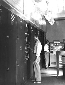
EDVAC, one of the first stored-program computers
Early computers such as the ENIAC had to be physically rewired to perform different tasks, which caused these machines to be called «fixed-program computers».[4] The «central processing unit» term has been in use since as early as 1955.[5][6] Since the term «CPU» is generally defined as a device for software (computer program) execution, the earliest devices that could rightly be called CPUs came with the advent of the stored-program computer.
The idea of a stored-program computer had been already present in the design of J. Presper Eckert and John William Mauchly’s ENIAC, but was initially omitted so that it could be finished sooner.[7] On June 30, 1945, before ENIAC was made, mathematician John von Neumann distributed the paper entitled First Draft of a Report on the EDVAC. It was the outline of a stored-program computer that would eventually be completed in August 1949.[8] EDVAC was designed to perform a certain number of instructions (or operations) of various types. Significantly, the programs written for EDVAC were to be stored in high-speed computer memory rather than specified by the physical wiring of the computer.[9] This overcame a severe limitation of ENIAC, which was the considerable time and effort required to reconfigure the computer to perform a new task.[10] With von Neumann’s design, the program that EDVAC ran could be changed simply by changing the contents of the memory. EDVAC was not the first stored-program computer; the Manchester Baby, which was a small-scale experimental stored-program computer, ran its first program on 21 June 1948[11] and the Manchester Mark 1 ran its first program during the night of 16–17 June 1949.[12]
Early CPUs were custom designs used as part of a larger and sometimes distinctive computer.[13] However, this method of designing custom CPUs for a particular application has largely given way to the development of multi-purpose processors produced in large quantities. This standardization began in the era of discrete transistor mainframes and minicomputers and has rapidly accelerated with the popularization of the integrated circuit (IC). The IC has allowed increasingly complex CPUs to be designed and manufactured to tolerances on the order of nanometers.[14] Both the miniaturization and standardization of CPUs have increased the presence of digital devices in modern life far beyond the limited application of dedicated computing machines. Modern microprocessors appear in electronic devices ranging from automobiles[15] to cellphones,[16] and sometimes even in toys.[17][18]
While von Neumann is most often credited with the design of the stored-program computer because of his design of EDVAC, and the design became known as the von Neumann architecture, others before him, such as Konrad Zuse, had suggested and implemented similar ideas.[19] The so-called Harvard architecture of the Harvard Mark I, which was completed before EDVAC,[20][21] also used a stored-program design using punched paper tape rather than electronic memory.[22] The key difference between the von Neumann and Harvard architectures is that the latter separates the storage and treatment of CPU instructions and data, while the former uses the same memory space for both.[23] Most modern CPUs are primarily von Neumann in design, but CPUs with the Harvard architecture are seen as well, especially in embedded applications; for instance, the Atmel AVR microcontrollers are Harvard architecture processors.[24]
Relays and vacuum tubes (thermionic tubes) were commonly used as switching elements;[25][26] a useful computer requires thousands or tens of thousands of switching devices. The overall speed of a system is dependent on the speed of the switches. Vacuum-tube computers such as EDVAC tended to average eight hours between failures, whereas relay computers like the (slower, but earlier) Harvard Mark I failed very rarely.[6] In the end, tube-based CPUs became dominant because the significant speed advantages afforded generally outweighed the reliability problems. Most of these early synchronous CPUs ran at low clock rates compared to modern microelectronic designs. Clock signal frequencies ranging from 100 kHz to 4 MHz were very common at this time, limited largely by the speed of the switching devices they were built with.[27]
Transistor CPUs[edit]

IBM PowerPC 604e processor
The design complexity of CPUs increased as various technologies facilitated building smaller and more reliable electronic devices. The first such improvement came with the advent of the transistor. Transistorized CPUs during the 1950s and 1960s no longer had to be built out of bulky, unreliable and fragile switching elements like vacuum tubes and relays.[28] With this improvement, more complex and reliable CPUs were built onto one or several printed circuit boards containing discrete (individual) components.
In 1964, IBM introduced its IBM System/360 computer architecture that was used in a series of computers capable of running the same programs with different speed and performance.[29] This was significant at a time when most electronic computers were incompatible with one another, even those made by the same manufacturer. To facilitate this improvement, IBM used the concept of a microprogram (often called «microcode»), which still sees widespread usage in modern CPUs.[30] The System/360 architecture was so popular that it dominated the mainframe computer market for decades and left a legacy that is still continued by similar modern computers like the IBM zSeries.[31][32] In 1965, Digital Equipment Corporation (DEC) introduced another influential computer aimed at the scientific and research markets, the PDP-8.[33]

Fujitsu board with SPARC64 VIIIfx processors
Transistor-based computers had several distinct advantages over their predecessors. Aside from facilitating increased reliability and lower power consumption, transistors also allowed CPUs to operate at much higher speeds because of the short switching time of a transistor in comparison to a tube or relay.[34] The increased reliability and dramatically increased speed of the switching elements (which were almost exclusively transistors by this time); CPU clock rates in the tens of megahertz were easily obtained during this period.[35] Additionally, while discrete transistor and IC CPUs were in heavy usage, new high-performance designs like single instruction, multiple data (SIMD) vector processors began to appear.[36] These early experimental designs later gave rise to the era of specialized supercomputers like those made by Cray Inc and Fujitsu Ltd.[36]
Small-scale integration CPUs[edit]

During this period, a method of manufacturing many interconnected transistors in a compact space was developed. The integrated circuit (IC) allowed a large number of transistors to be manufactured on a single semiconductor-based die, or «chip». At first, only very basic non-specialized digital circuits such as NOR gates were miniaturized into ICs.[37] CPUs based on these «building block» ICs are generally referred to as «small-scale integration» (SSI) devices. SSI ICs, such as the ones used in the Apollo Guidance Computer, usually contained up to a few dozen transistors. To build an entire CPU out of SSI ICs required thousands of individual chips, but still consumed much less space and power than earlier discrete transistor designs.[38]
IBM’s System/370, follow-on to the System/360, used SSI ICs rather than Solid Logic Technology discrete-transistor modules.[39][40] DEC’s PDP-8/I and KI10 PDP-10 also switched from the individual transistors used by the PDP-8 and PDP-10 to SSI ICs,[41] and their extremely popular PDP-11 line was originally built with SSI ICs but was eventually implemented with LSI components once these became practical.
Large-scale integration CPUs[edit]
Lee Boysel published influential articles, including a 1967 «manifesto», which described how to build the equivalent of a 32-bit mainframe computer from a relatively small number of large-scale integration circuits (LSI).[42][43] The only way to build LSI chips, which are chips with a hundred or more gates, was to build them using a metal–oxide–semiconductor (MOS) semiconductor manufacturing process (either PMOS logic, NMOS logic, or CMOS logic). However, some companies continued to build processors out of bipolar transistor–transistor logic (TTL) chips because bipolar junction transistors were faster than MOS chips up until the 1970s (a few companies such as Datapoint continued to build processors out of TTL chips until the early 1980s).[43] In the 1960s, MOS ICs were slower and initially considered useful only in applications that required low power.[44][45] Following the development of silicon-gate MOS technology by Federico Faggin at Fairchild Semiconductor in 1968, MOS ICs largely replaced bipolar TTL as the standard chip technology in the early 1970s.[46]
As the microelectronic technology advanced, an increasing number of transistors were placed on ICs, decreasing the number of individual ICs needed for a complete CPU. MSI and LSI ICs increased transistor counts to hundreds, and then thousands. By 1968, the number of ICs required to build a complete CPU had been reduced to 24 ICs of eight different types, with each IC containing roughly 1000 MOSFETs.[47] In stark contrast with its SSI and MSI predecessors, the first LSI implementation of the PDP-11 contained a CPU composed of only four LSI integrated circuits.[48]
Microprocessors[edit]


Inside of a laptop, with the CPU removed from socket
Since microprocessors were first introduced they have almost completely overtaken all other central processing unit implementation methods. The first commercially available microprocessor, made in 1971, was the Intel 4004, and the first widely used microprocessor, made in 1974, was the Intel 8080. Mainframe and minicomputer manufacturers of the time launched proprietary IC development programs to upgrade their older computer architectures, and eventually produced instruction set compatible microprocessors that were backward-compatible with their older hardware and software. Combined with the advent and eventual success of the ubiquitous personal computer, the term CPU is now applied almost exclusively[a] to microprocessors. Several CPUs (denoted cores) can be combined in a single processing chip.[49]
Previous generations of CPUs were implemented as discrete components and numerous small integrated circuits (ICs) on one or more circuit boards.[50] Microprocessors, on the other hand, are CPUs manufactured on a very small number of ICs; usually just one.[51] The overall smaller CPU size, as a result of being implemented on a single die, means faster switching time because of physical factors like decreased gate parasitic capacitance.[52][53] This has allowed synchronous microprocessors to have clock rates ranging from tens of megahertz to several gigahertz. Additionally, the ability to construct exceedingly small transistors on an IC has increased the complexity and number of transistors in a single CPU many fold. This widely observed trend is described by Moore’s law, which had proven to be a fairly accurate predictor of the growth of CPU (and other IC) complexity until 2016.[54][55]
While the complexity, size, construction and general form of CPUs have changed enormously since 1950,[56] the basic design and function has not changed much at all. Almost all common CPUs today can be very accurately described as von Neumann stored-program machines.[57][b] As Moore’s law no longer holds, concerns have arisen about the limits of integrated circuit transistor technology. Extreme miniaturization of electronic gates is causing the effects of phenomena like electromigration and subthreshold leakage to become much more significant.[59][60] These newer concerns are among the many factors causing researchers to investigate new methods of computing such as the quantum computer, as well as to expand the usage of parallelism and other methods that extend the usefulness of the classical von Neumann model.
Operation[edit]
The fundamental operation of most CPUs, regardless of the physical form they take, is to execute a sequence of stored instructions that is called a program. The instructions to be executed are kept in some kind of computer memory. Nearly all CPUs follow the fetch, decode and execute steps in their operation, which are collectively known as the instruction cycle.
After the execution of an instruction, the entire process repeats, with the next instruction cycle normally fetching the next-in-sequence instruction because of the incremented value in the program counter. If a jump instruction was executed, the program counter will be modified to contain the address of the instruction that was jumped to and program execution continues normally. In more complex CPUs, multiple instructions can be fetched, decoded and executed simultaneously. This section describes what is generally referred to as the «classic RISC pipeline», which is quite common among the simple CPUs used in many electronic devices (often called microcontrollers). It largely ignores the important role of CPU cache, and therefore the access stage of the pipeline.
Some instructions manipulate the program counter rather than producing result data directly; such instructions are generally called «jumps» and facilitate program behavior like loops, conditional program execution (through the use of a conditional jump), and existence of functions.[c] In some processors, some other instructions change the state of bits in a «flags» register. These flags can be used to influence how a program behaves, since they often indicate the outcome of various operations. For example, in such processors a «compare» instruction evaluates two values and sets or clears bits in the flags register to indicate which one is greater or whether they are equal; one of these flags could then be used by a later jump instruction to determine program flow.
Fetch[edit]
Fetch involves retrieving an instruction (which is represented by a number or sequence of numbers) from program memory. The instruction’s location (address) in program memory is determined by the program counter (PC; called the «instruction pointer» in Intel x86 microprocessors), which stores a number that identifies the address of the next instruction to be fetched. After an instruction is fetched, the PC is incremented by the length of the instruction so that it will contain the address of the next instruction in the sequence.[d] Often, the instruction to be fetched must be retrieved from relatively slow memory, causing the CPU to stall while waiting for the instruction to be returned. This issue is largely addressed in modern processors by caches and pipeline architectures (see below).
Decode[edit]
The instruction that the CPU fetches from memory determines what the CPU will do. In the decode step, performed by binary decoder circuitry known as the instruction decoder, the instruction is converted into signals that control other parts of the CPU.
The way in which the instruction is interpreted is defined by the CPU’s instruction set architecture (ISA).[e] Often, one group of bits (that is, a «field») within the instruction, called the opcode, indicates which operation is to be performed, while the remaining fields usually provide supplemental information required for the operation, such as the operands. Those operands may be specified as a constant value (called an immediate value), or as the location of a value that may be a processor register or a memory address, as determined by some addressing mode.
In some CPU designs the instruction decoder is implemented as a hardwired, unchangeable binary decoder circuit. In others, a microprogram is used to translate instructions into sets of CPU configuration signals that are applied sequentially over multiple clock pulses. In some cases the memory that stores the microprogram is rewritable, making it possible to change the way in which the CPU decodes instructions.
Execute[edit]
After the fetch and decode steps, the execute step is performed. Depending on the CPU architecture, this may consist of a single action or a sequence of actions. During each action, control signals electrically enable or disable various parts of the CPU so they can perform all or part of the desired operation. The action is then completed, typically in response to a clock pulse. Very often the results are written to an internal CPU register for quick access by subsequent instructions. In other cases results may be written to slower, but less expensive and higher capacity main memory.
For example, if an addition instruction is to be executed, registers containing operands (numbers to be summed) are activated, as are the parts of the arithmetic logic unit (ALU) that perform addition. When the clock pulse occurs, the operands flow from the source registers into the ALU, and the sum appears at its output. On subsequent clock pulses, other components are enabled (and disabled) to move the output (the sum of the operation) to storage (e.g., a register or memory). If the resulting sum is too large (i.e., it is larger than the ALU’s output word size), an arithmetic overflow flag will be set, influencing the next operation.
Structure and implementation[edit]

Block diagram of a basic uniprocessor-CPU computer. Black lines indicate data flow, whereas red lines indicate control flow; arrows indicate flow directions.
Hardwired into a CPU’s circuitry is a set of basic operations it can perform, called an instruction set. Such operations may involve, for example, adding or subtracting two numbers, comparing two numbers, or jumping to a different part of a program. Each instruction is represented by a unique combination of bits, known as the machine language opcode. While processing an instruction, the CPU decodes the opcode (via a binary decoder) into control signals, which orchestrate the behavior of the CPU. A complete machine language instruction consists of an opcode and, in many cases, additional bits that specify arguments for the operation (for example, the numbers to be summed in the case of an addition operation). Going up the complexity scale, a machine language program is a collection of machine language instructions that the CPU executes.
The actual mathematical operation for each instruction is performed by a combinational logic circuit within the CPU’s processor known as the arithmetic–logic unit or ALU. In general, a CPU executes an instruction by fetching it from memory, using its ALU to perform an operation, and then storing the result to memory. Beside the instructions for integer mathematics and logic operations, various other machine instructions exist, such as those for loading data from memory and storing it back, branching operations, and mathematical operations on floating-point numbers performed by the CPU’s floating-point unit (FPU).[61]
Control unit[edit]
The control unit (CU) is a component of the CPU that directs the operation of the processor. It tells the computer’s memory, arithmetic and logic unit and input and output devices how to respond to the instructions that have been sent to the processor.
It directs the operation of the other units by providing timing and control signals. Most computer resources are managed by the CU. It directs the flow of data between the CPU and the other devices. John von Neumann included the control unit as part of the von Neumann architecture. In modern computer designs, the control unit is typically an internal part of the CPU with its overall role and operation unchanged since its introduction.[62]
Arithmetic logic unit[edit]

Symbolic representation of an ALU and its input and output signals
The arithmetic logic unit (ALU) is a digital circuit within the processor that performs integer arithmetic and bitwise logic operations. The inputs to the ALU are the data words to be operated on (called operands), status information from previous operations, and a code from the control unit indicating which operation to perform. Depending on the instruction being executed, the operands may come from internal CPU registers, external memory, or constants generated by the ALU itself.
When all input signals have settled and propagated through the ALU circuitry, the result of the performed operation appears at the ALU’s outputs. The result consists of both a data word, which may be stored in a register or memory, and status information that is typically stored in a special, internal CPU register reserved for this purpose.
Address generation unit[edit]
The address generation unit (AGU), sometimes also called the address computation unit (ACU),[63] is an execution unit inside the CPU that calculates addresses used by the CPU to access main memory. By having address calculations handled by separate circuitry that operates in parallel with the rest of the CPU, the number of CPU cycles required for executing various machine instructions can be reduced, bringing performance improvements.
While performing various operations, CPUs need to calculate memory addresses required for fetching data from the memory; for example, in-memory positions of array elements must be calculated before the CPU can fetch the data from actual memory locations. Those address-generation calculations involve different integer arithmetic operations, such as addition, subtraction, modulo operations, or bit shifts. Often, calculating a memory address involves more than one general-purpose machine instruction, which do not necessarily decode and execute quickly. By incorporating an AGU into a CPU design, together with introducing specialized instructions that use the AGU, various address-generation calculations can be offloaded from the rest of the CPU, and can often be executed quickly in a single CPU cycle.
Capabilities of an AGU depend on a particular CPU and its architecture. Thus, some AGUs implement and expose more address-calculation operations, while some also include more advanced specialized instructions that can operate on multiple operands at a time. Some CPU architectures include multiple AGUs so more than one address-calculation operation can be executed simultaneously, which brings further performance improvements due to the superscalar nature of advanced CPU designs. For example, Intel incorporates multiple AGUs into its Sandy Bridge and Haswell microarchitectures, which increase bandwidth of the CPU memory subsystem by allowing multiple memory-access instructions to be executed in parallel.
Memory management unit (MMU)[edit]
Many microprocessors (in smartphones and desktop, laptop, server computers) have a memory management unit, translating logical addresses into physical RAM addresses, providing memory protection and paging abilities, useful for virtual memory. Simpler processors, especially microcontrollers, usually don’t include an MMU.
Cache[edit]
A CPU cache[64] is a hardware cache used by the central processing unit (CPU) of a computer to reduce the average cost (time or energy) to access data from the main memory. A cache is a smaller, faster memory, closer to a processor core, which stores copies of the data from frequently used main memory locations. Most CPUs have different independent caches, including instruction and data caches, where the data cache is usually organized as a hierarchy of more cache levels (L1, L2, L3, L4, etc.).
All modern (fast) CPUs (with few specialized exceptions[f]) have multiple levels of CPU caches. The first CPUs that used a cache had only one level of cache; unlike later level 1 caches, it was not split into L1d (for data) and L1i (for instructions). Almost all current CPUs with caches have a split L1 cache. They also have L2 caches and, for larger processors, L3 caches as well. The L2 cache is usually not split and acts as a common repository for the already split L1 cache. Every core of a multi-core processor has a dedicated L2 cache and is usually not shared between the cores. The L3 cache, and higher-level caches, are shared between the cores and are not split. An L4 cache is currently uncommon, and is generally on dynamic random-access memory (DRAM), rather than on static random-access memory (SRAM), on a separate die or chip. That was also the case historically with L1, while bigger chips have allowed integration of it and generally all cache levels, with the possible exception of the last level. Each extra level of cache tends to be bigger and be optimized differently.
Other types of caches exist (that are not counted towards the «cache size» of the most important caches mentioned above), such as the translation lookaside buffer (TLB) that is part of the memory management unit (MMU) that most CPUs have.
Caches are generally sized in powers of two: 2, 8, 16 etc. KiB or MiB (for larger non-L1) sizes, although the IBM z13 has a 96 KiB L1 instruction cache.[65]
Clock rate[edit]
Most CPUs are synchronous circuits, which means they employ a clock signal to pace their sequential operations. The clock signal is produced by an external oscillator circuit that generates a consistent number of pulses each second in the form of a periodic square wave. The frequency of the clock pulses determines the rate at which a CPU executes instructions and, consequently, the faster the clock, the more instructions the CPU will execute each second.
To ensure proper operation of the CPU, the clock period is longer than the maximum time needed for all signals to propagate (move) through the CPU. In setting the clock period to a value well above the worst-case propagation delay, it is possible to design the entire CPU and the way it moves data around the «edges» of the rising and falling clock signal. This has the advantage of simplifying the CPU significantly, both from a design perspective and a component-count perspective. However, it also carries the disadvantage that the entire CPU must wait on its slowest elements, even though some portions of it are much faster. This limitation has largely been compensated for by various methods of increasing CPU parallelism (see below).
However, architectural improvements alone do not solve all of the drawbacks of globally synchronous CPUs. For example, a clock signal is subject to the delays of any other electrical signal. Higher clock rates in increasingly complex CPUs make it more difficult to keep the clock signal in phase (synchronized) throughout the entire unit. This has led many modern CPUs to require multiple identical clock signals to be provided to avoid delaying a single signal significantly enough to cause the CPU to malfunction. Another major issue, as clock rates increase dramatically, is the amount of heat that is dissipated by the CPU. The constantly changing clock causes many components to switch regardless of whether they are being used at that time. In general, a component that is switching uses more energy than an element in a static state. Therefore, as clock rate increases, so does energy consumption, causing the CPU to require more heat dissipation in the form of CPU cooling solutions.
One method of dealing with the switching of unneeded components is called clock gating, which involves turning off the clock signal to unneeded components (effectively disabling them). However, this is often regarded as difficult to implement and therefore does not see common usage outside of very low-power designs. One notable recent CPU design that uses extensive clock gating is the IBM PowerPC-based Xenon used in the Xbox 360; that way, power requirements of the Xbox 360 are greatly reduced.[66]
Clockless CPUs[edit]
Another method of addressing some of the problems with a global clock signal is the removal of the clock signal altogether. While removing the global clock signal makes the design process considerably more complex in many ways, asynchronous (or clockless) designs carry marked advantages in power consumption and heat dissipation in comparison with similar synchronous designs. While somewhat uncommon, entire asynchronous CPUs have been built without using a global clock signal. Two notable examples of this are the ARM compliant AMULET and the MIPS R3000 compatible MiniMIPS.[67]
Rather than totally removing the clock signal, some CPU designs allow certain portions of the device to be asynchronous, such as using asynchronous ALUs in conjunction with superscalar pipelining to achieve some arithmetic performance gains. While it is not altogether clear whether totally asynchronous designs can perform at a comparable or better level than their synchronous counterparts, it is evident that they do at least excel in simpler math operations. This, combined with their excellent power consumption and heat dissipation properties, makes them very suitable for embedded computers.[68]
Voltage regulator module[edit]
Many modern CPUs have a die-integrated power managing module which regulates on-demand voltage supply to the CPU circuitry allowing it to keep balance between performance and power consumption.
Integer range[edit]
Every CPU represents numerical values in a specific way. For example, some early digital computers represented numbers as familiar decimal (base 10) numeral system values, and others have employed more unusual representations such as ternary (base three). Nearly all modern CPUs represent numbers in binary form, with each digit being represented by some two-valued physical quantity such as a «high» or «low» voltage.[g]

A six-bit word containing the binary encoded representation of decimal value 40. Most modern CPUs employ word sizes that are a power of two, for example 8, 16, 32 or 64 bits.
Related to numeric representation is the size and precision of integer numbers that a CPU can represent. In the case of a binary CPU, this is measured by the number of bits (significant digits of a binary encoded integer) that the CPU can process in one operation, which is commonly called word size, bit width, data path width, integer precision, or integer size. A CPU’s integer size determines the range of integer values it can directly operate on.[h] For example, an 8-bit CPU can directly manipulate integers represented by eight bits, which have a range of 256 (28) discrete integer values.
Integer range can also affect the number of memory locations the CPU can directly address (an address is an integer value representing a specific memory location). For example, if a binary CPU uses 32 bits to represent a memory address then it can directly address 232 memory locations. To circumvent this limitation and for various other reasons, some CPUs use mechanisms (such as bank switching) that allow additional memory to be addressed.
CPUs with larger word sizes require more circuitry and consequently are physically larger, cost more and consume more power (and therefore generate more heat). As a result, smaller 4- or 8-bit microcontrollers are commonly used in modern applications even though CPUs with much larger word sizes (such as 16, 32, 64, even 128-bit) are available. When higher performance is required, however, the benefits of a larger word size (larger data ranges and address spaces) may outweigh the disadvantages. A CPU can have internal data paths shorter than the word size to reduce size and cost. For example, even though the IBM System/360 instruction set was a 32-bit instruction set, the System/360 Model 30 and Model 40 had 8-bit data paths in the arithmetic logical unit, so that a 32-bit add required four cycles, one for each 8 bits of the operands, and, even though the Motorola 68000 series instruction set was a 32-bit instruction set, the Motorola 68000 and Motorola 68010 had 16-bit data paths in the arithmetic logical unit, so that a 32-bit add required two cycles.
To gain some of the advantages afforded by both lower and higher bit lengths, many instruction sets have different bit widths for integer and floating-point data, allowing CPUs implementing that instruction set to have different bit widths for different portions of the device. For example, the IBM System/360 instruction set was primarily 32 bit, but supported 64-bit floating-point values to facilitate greater accuracy and range in floating-point numbers.[30] The System/360 Model 65 had an 8-bit adder for decimal and fixed-point binary arithmetic and a 60-bit adder for floating-point arithmetic.[69] Many later CPU designs use similar mixed bit width, especially when the processor is meant for general-purpose usage where a reasonable balance of integer and floating-point capability is required.
Parallelism[edit]

Model of a subscalar CPU, in which it takes fifteen clock cycles to complete three instructions
The description of the basic operation of a CPU offered in the previous section describes the simplest form that a CPU can take. This type of CPU, usually referred to as subscalar, operates on and executes one instruction on one or two pieces of data at a time, that is less than one instruction per clock cycle (IPC < 1).
This process gives rise to an inherent inefficiency in subscalar CPUs. Since only one instruction is executed at a time, the entire CPU must wait for that instruction to complete before proceeding to the next instruction. As a result, the subscalar CPU gets «hung up» on instructions which take more than one clock cycle to complete execution. Even adding a second execution unit (see below) does not improve performance much; rather than one pathway being hung up, now two pathways are hung up and the number of unused transistors is increased. This design, wherein the CPU’s execution resources can operate on only one instruction at a time, can only possibly reach scalar performance (one instruction per clock cycle, IPC = 1). However, the performance is nearly always subscalar (less than one instruction per clock cycle, IPC < 1).
Attempts to achieve scalar and better performance have resulted in a variety of design methodologies that cause the CPU to behave less linearly and more in parallel. When referring to parallelism in CPUs, two terms are generally used to classify these design techniques:
- instruction-level parallelism (ILP), which seeks to increase the rate at which instructions are executed within a CPU (that is, to increase the use of on-die execution resources);
- task-level parallelism (TLP), which purposes to increase the number of threads or processes that a CPU can execute simultaneously.
Each methodology differs both in the ways in which they are implemented, as well as the relative effectiveness they afford in increasing the CPU’s performance for an application.[i]
Instruction-level parallelism[edit]

Basic five-stage pipeline. In the best case scenario, this pipeline can sustain a completion rate of one instruction per clock cycle.
One of the simplest methods for increased parallelism is to begin the first steps of instruction fetching and decoding before the prior instruction finishes executing. This is a technique known as instruction pipelining, and is used in almost all modern general-purpose CPUs. Pipelining allows multiple instruction to be executed at a time by breaking the execution pathway into discrete stages. This separation can be compared to an assembly line, in which an instruction is made more complete at each stage until it exits the execution pipeline and is retired.
Pipelining does, however, introduce the possibility for a situation where the result of the previous operation is needed to complete the next operation; a condition often termed data dependency conflict. Therefore pipelined processors must check for these sorts of conditions and delay a portion of the pipeline if necessary. A pipelined processor can become very nearly scalar, inhibited only by pipeline stalls (an instruction spending more than one clock cycle in a stage).

A simple superscalar pipeline. By fetching and dispatching two instructions at a time, a maximum of two instructions per clock cycle can be completed.
Improvements in instruction pipelining led to further decreases in the idle time of CPU components. Designs that are said to be superscalar include a long instruction pipeline and multiple identical execution units, such as load–store units, arithmetic–logic units, floating-point units and address generation units.[70] In a superscalar pipeline, instructions are read and passed to a dispatcher, which decides whether or not the instructions can be executed in parallel (simultaneously). If so, they are dispatched to execution units, resulting in their simultaneous execution. In general, the number of instructions that a superscalar CPU will complete in a cycle is dependent on the number of instructions it is able to dispatch simultaneously to execution units.
Most of the difficulty in the design of a superscalar CPU architecture lies in creating an effective dispatcher. The dispatcher needs to be able to quickly determine whether instructions can be executed in parallel, as well as dispatch them in such a way as to keep as many execution units busy as possible. This requires that the instruction pipeline is filled as often as possible and requires significant amounts of CPU cache. It also makes hazard-avoiding techniques like branch prediction, speculative execution, register renaming, out-of-order execution and transactional memory crucial to maintaining high levels of performance. By attempting to predict which branch (or path) a conditional instruction will take, the CPU can minimize the number of times that the entire pipeline must wait until a conditional instruction is completed. Speculative execution often provides modest performance increases by executing portions of code that may not be needed after a conditional operation completes. Out-of-order execution somewhat rearranges the order in which instructions are executed to reduce delays due to data dependencies. Also in case of single instruction stream, multiple data stream—a case when a lot of data from the same type has to be processed—, modern processors can disable parts of the pipeline so that when a single instruction is executed many times, the CPU skips the fetch and decode phases and thus greatly increases performance on certain occasions, especially in highly monotonous program engines such as video creation software and photo processing.
When just a fraction of the CPU is superscalar, the part that is not suffers a performance penalty due to scheduling stalls. The Intel P5 Pentium had two superscalar ALUs which could accept one instruction per clock cycle each, but its FPU could not. Thus the P5 was integer superscalar but not floating point superscalar. Intel’s successor to the P5 architecture, P6, added superscalar abilities to its floating-point features.
Simple pipelining and superscalar design increase a CPU’s ILP by allowing it to execute instructions at rates surpassing one instruction per clock cycle. Most modern CPU designs are at least somewhat superscalar, and nearly all general purpose CPUs designed in the last decade are superscalar. In later years some of the emphasis in designing high-ILP computers has been moved out of the CPU’s hardware and into its software interface, or instruction set architecture (ISA). The strategy of the very long instruction word (VLIW) causes some ILP to become implied directly by the software, reducing the CPU’s work in boosting ILP and thereby reducing design complexity.
Task-level parallelism[edit]
Another strategy of achieving performance is to execute multiple threads or processes in parallel. This area of research is known as parallel computing.[71] In Flynn’s taxonomy, this strategy is known as multiple instruction stream, multiple data stream (MIMD).[72]
One technology used for this purpose was multiprocessing (MP).[73] The initial flavor of this technology is known as symmetric multiprocessing (SMP), where a small number of CPUs share a coherent view of their memory system. In this scheme, each CPU has additional hardware to maintain a constantly up-to-date view of memory. By avoiding stale views of memory, the CPUs can cooperate on the same program and programs can migrate from one CPU to another. To increase the number of cooperating CPUs beyond a handful, schemes such as non-uniform memory access (NUMA) and directory-based coherence protocols were introduced in the 1990s. SMP systems are limited to a small number of CPUs while NUMA systems have been built with thousands of processors. Initially, multiprocessing was built using multiple discrete CPUs and boards to implement the interconnect between the processors. When the processors and their interconnect are all implemented on a single chip, the technology is known as chip-level multiprocessing (CMP) and the single chip as a multi-core processor.
It was later recognized that finer-grain parallelism existed with a single program. A single program might have several threads (or functions) that could be executed separately or in parallel. Some of the earliest examples of this technology implemented input/output processing such as direct memory access as a separate thread from the computation thread. A more general approach to this technology was introduced in the 1970s when systems were designed to run multiple computation threads in parallel. This technology is known as multi-threading (MT). This approach is considered more cost-effective than multiprocessing, as only a small number of components within a CPU is replicated to support MT as opposed to the entire CPU in the case of MP. In MT, the execution units and the memory system including the caches are shared among multiple threads. The downside of MT is that the hardware support for multithreading is more visible to software than that of MP and thus supervisor software like operating systems have to undergo larger changes to support MT. One type of MT that was implemented is known as temporal multithreading, where one thread is executed until it is stalled waiting for data to return from external memory. In this scheme, the CPU would then quickly context switch to another thread which is ready to run, the switch often done in one CPU clock cycle, such as the UltraSPARC T1. Another type of MT is simultaneous multithreading, where instructions from multiple threads are executed in parallel within one CPU clock cycle.
For several decades from the 1970s to early 2000s, the focus in designing high performance general purpose CPUs was largely on achieving high ILP through technologies such as pipelining, caches, superscalar execution, out-of-order execution, etc. This trend culminated in large, power-hungry CPUs such as the Intel Pentium 4. By the early 2000s, CPU designers were thwarted from achieving higher performance from ILP techniques due to the growing disparity between CPU operating frequencies and main memory operating frequencies as well as escalating CPU power dissipation owing to more esoteric ILP techniques.
CPU designers then borrowed ideas from commercial computing markets such as transaction processing, where the aggregate performance of multiple programs, also known as throughput computing, was more important than the performance of a single thread or process.
This reversal of emphasis is evidenced by the proliferation of dual and more core processor designs and notably, Intel’s newer designs resembling its less superscalar P6 architecture. Late designs in several processor families exhibit CMP, including the x86-64 Opteron and Athlon 64 X2, the SPARC UltraSPARC T1, IBM POWER4 and POWER5, as well as several video game console CPUs like the Xbox 360’s triple-core PowerPC design, and the PlayStation 3’s 7-core Cell microprocessor.
Data parallelism[edit]
A less common but increasingly important paradigm of processors (and indeed, computing in general) deals with data parallelism. The processors discussed earlier are all referred to as some type of scalar device.[j] As the name implies, vector processors deal with multiple pieces of data in the context of one instruction. This contrasts with scalar processors, which deal with one piece of data for every instruction. Using Flynn’s taxonomy, these two schemes of dealing with data are generally referred to as single instruction stream, multiple data stream (SIMD) and single instruction stream, single data stream (SISD), respectively. The great utility in creating processors that deal with vectors of data lies in optimizing tasks that tend to require the same operation (for example, a sum or a dot product) to be performed on a large set of data. Some classic examples of these types of tasks include multimedia applications (images, video and sound), as well as many types of scientific and engineering tasks. Whereas a scalar processor must complete the entire process of fetching, decoding and executing each instruction and value in a set of data, a vector processor can perform a single operation on a comparatively large set of data with one instruction. This is only possible when the application tends to require many steps which apply one operation to a large set of data.
Most early vector processors, such as the Cray-1, were associated almost exclusively with scientific research and cryptography applications. However, as multimedia has largely shifted to digital media, the need for some form of SIMD in general-purpose processors has become significant. Shortly after inclusion of floating-point units started to become commonplace in general-purpose processors, specifications for and implementations of SIMD execution units also began to appear for general-purpose processors.[when?] Some of these early SIMD specifications – like HP’s Multimedia Acceleration eXtensions (MAX) and Intel’s MMX – were integer-only. This proved to be a significant impediment for some software developers, since many of the applications that benefit from SIMD primarily deal with floating-point numbers. Progressively, developers refined and remade these early designs into some of the common modern SIMD specifications, which are usually associated with one instruction set architecture (ISA). Some notable modern examples include Intel’s Streaming SIMD Extensions (SSE) and the PowerPC-related AltiVec (also known as VMX).[k]
Hardware performance counter[edit]
Many modern architectures (including embedded ones) often include hardware performance counters (HPC), which enables low-level (instruction-level) collection, benchmarking, debugging or analysis of running software metrics.[74][75] HPC may also be used to discover and analyze unusual or suspicious activity of the software, such as return-oriented programming (ROP) or sigreturn-oriented programming (SROP) exploits etc.[76] This is usually done by software-security teams to assess and find malicious binary programs.
Many major vendors (such as IBM, Intel, AMD, and Arm etc.) provide software interfaces (usually written in C/C++) that can be used to collected data from CPUs registers in order to get metrics.[77] Operating system vendors also provide software like perf (Linux) to record, benchmark, or trace CPU events running kernels and applications.
Virtual CPUs[edit]
|
This section needs expansion. You can help by adding to it. (September 2016) |
Cloud computing can involve subdividing CPU operation into virtual central processing units[78] (vCPUs[79]).
A host is the virtual equivalent of a physical machine, on which a virtual system is operating.[80] When there are several physical machines operating in tandem and managed as a whole, the grouped computing and memory resources form a cluster. In some systems, it is possible to dynamically add and remove from a cluster. Resources available at a host and cluster level can be partitioned out into resources pools with fine granularity.
Performance[edit]
The performance or speed of a processor depends on, among many other factors, the clock rate (generally given in multiples of hertz) and the instructions per clock (IPC), which together are the factors for the instructions per second (IPS) that the CPU can perform.[81]
Many reported IPS values have represented «peak» execution rates on artificial instruction sequences with few branches, whereas realistic workloads consist of a mix of instructions and applications, some of which take longer to execute than others. The performance of the memory hierarchy also greatly affects processor performance, an issue barely considered in MIPS calculations. Because of these problems, various standardized tests, often called «benchmarks» for this purpose—such as SPECint—have been developed to attempt to measure the real effective performance in commonly used applications.
Processing performance of computers is increased by using multi-core processors, which essentially is plugging two or more individual processors (called cores in this sense) into one integrated circuit.[82] Ideally, a dual core processor would be nearly twice as powerful as a single core processor. In practice, the performance gain is far smaller, only about 50%, due to imperfect software algorithms and implementation.[83] Increasing the number of cores in a processor (i.e. dual-core, quad-core, etc.) increases the workload that can be handled. This means that the processor can now handle numerous asynchronous events, interrupts, etc. which can take a toll on the CPU when overwhelmed. These cores can be thought of as different floors in a processing plant, with each floor handling a different task. Sometimes, these cores will handle the same tasks as cores adjacent to them if a single core is not enough to handle the information.
Due to specific capabilities of modern CPUs, such as simultaneous multithreading and uncore, which involve sharing of actual CPU resources while aiming at increased utilization, monitoring performance levels and hardware use gradually became a more complex task.[84] As a response, some CPUs implement additional hardware logic that monitors actual use of various parts of a CPU and provides various counters accessible to software; an example is Intel’s Performance Counter Monitor technology.[2]
See also[edit]
- Addressing mode
- AMD Accelerated Processing Unit
- Complex instruction set computer
- Computer bus
- Computer engineering
- CPU core voltage
- CPU socket
- Data processing unit
- Digital signal processor
- Graphics processing unit
- Comparison of instruction set architectures
- Protection ring
- Reduced instruction set computer
- Stream processing
- True Performance Index
- Tensor Processing Unit
- Wait state
Notes[edit]
- ^ Integrated circuits are now used to implement all CPUs, except for a few machines designed to withstand large electromagnetic pulses, say from a nuclear weapon.
- ^ The so-called «von Neumann» memo expounded the idea of stored programs,[58] which for example may be stored on punched cards, paper tape, or magnetic tape.
- ^ Some early computers, like the Harvard Mark I, did not support any kind of «jump» instruction, effectively limiting the complexity of the programs they could run. It is largely for this reason that these computers are often not considered to contain a proper CPU, despite their close similarity to stored-program computers.
- ^ Since the program counter counts memory addresses and not instructions, it is incremented by the number of memory units that the instruction word contains. In the case of simple fixed-length instruction word ISAs, this is always the same number. For example, a fixed-length 32-bit instruction word ISA that uses 8-bit memory words would always increment the PC by four (except in the case of jumps). ISAs that use variable-length instruction words increment the PC by the number of memory words corresponding to the last instruction’s length.
- ^ Because the instruction set architecture of a CPU is fundamental to its interface and usage, it is often used as a classification of the «type» of CPU. For example, a «PowerPC CPU» uses some variant of the PowerPC ISA. A system can execute a different ISA by running an emulator.
- ^ A few specialized CPUs, accelerators or microcontrollers do not have a cache. To be fast, if needed/wanted, they still have an on-chip scratchpad memory that has a similar function, while software managed. In e.g. microcontrollers it can be better for hard real-time use, to have that or at least no cache, as with one level of memory latencies of loads are predictable.
- ^ The physical concept of voltage is an analog one by nature, practically having an infinite range of possible values. For the purpose of physical representation of binary numbers, two specific ranges of voltages are defined, one for logic ‘0’ and another for logic ‘1’. These ranges are dictated by design considerations such as noise margins and characteristics of the devices used to create the CPU.
- ^ While a CPU’s integer size sets a limit on integer ranges, this can (and often is) overcome using a combination of software and hardware techniques. By using additional memory, software can represent integers many magnitudes larger than the CPU can. Sometimes the CPU’s instruction set will even facilitate operations on integers larger than it can natively represent by providing instructions to make large integer arithmetic relatively quick. This method of dealing with large integers is slower than utilizing a CPU with higher integer size, but is a reasonable trade-off in cases where natively supporting the full integer range needed would be cost-prohibitive. See Arbitrary-precision arithmetic for more details on purely software-supported arbitrary-sized integers.
- ^ Neither ILP nor TLP is inherently superior over the other; they are simply different means by which to increase CPU parallelism. As such, they both have advantages and disadvantages, which are often determined by the type of software that the processor is intended to run. High-TLP CPUs are often used in applications that lend themselves well to being split up into numerous smaller applications, so-called «embarrassingly parallel problems». Frequently, a computational problem that can be solved quickly with high TLP design strategies like symmetric multiprocessing takes significantly more time on high ILP devices like superscalar CPUs, and vice versa.
- ^ Earlier the term scalar was used to compare the IPC count afforded by various ILP methods. Here the term is used in the strictly mathematical sense to contrast with vectors. See scalar (mathematics) and vector (geometric).
- ^ Although SSE/SSE2/SSE3 have superseded MMX in Intel’s general-purpose processors, later IA-32 designs still support MMX. This is usually done by providing most of the MMX functionality with the same hardware that supports the much more expansive SSE instruction sets.
References[edit]
- ^ Kuck, David (1978). Computers and Computations, Vol 1. John Wiley & Sons, Inc. p. 12. ISBN 978-0471027164.
- ^ a b Thomas Willhalm; Roman Dementiev; Patrick Fay (December 18, 2014). «Intel Performance Counter Monitor – A better way to measure CPU utilization». software.intel.com. Archived from the original on February 22, 2017. Retrieved February 17, 2015.
- ^ Liebowitz, Kusek, Spies, Matt, Christopher, Rynardt (2014). VMware vSphere Performance: Designing CPU, Memory, Storage, and Networking for Performance-Intensive Workloads. Wiley. p. 68. ISBN 978-1-118-00819-5.
{{cite book}}: CS1 maint: multiple names: authors list (link) - ^ Regan, Gerard (2008). A Brief History of Computing. p. 66. ISBN 978-1848000834. Retrieved 26 November 2014.
- ^ Weik, Martin H. (1955). «A Survey of Domestic Electronic Digital Computing Systems». Ballistic Research Laboratory. Archived from the original on 2021-01-26. Retrieved 2020-11-15.
- ^ a b Weik, Martin H. (1961). «A Third Survey of Domestic Electronic Digital Computing Systems». Ballistic Research Laboratory. Archived from the original on 2017-09-11. Retrieved 2005-12-16.
- ^ «Bit By Bit». Haverford College. Archived from the original on October 13, 2012. Retrieved August 1, 2015.
- ^ «First Draft of a Report on the EDVAC» (PDF). Moore School of Electrical Engineering, University of Pennsylvania. 1945. Archived (PDF) from the original on 2021-03-09. Retrieved 2018-03-31.
- ^ Stanford University. «The Modern History of Computing». The Stanford Encyclopedia of Philosophy. Archived from the original on March 3, 2017. Retrieved September 25, 2015.
- ^ «ENIAC’s Birthday». The MIT Press. February 9, 2016. Archived from the original on October 17, 2018. Retrieved October 17, 2018.
- ^ Enticknap, Nicholas (Summer 1998), «Computing’s Golden Jubilee», Resurrection, The Computer Conservation Society (20), ISSN 0958-7403, archived from the original on 17 March 2019, retrieved 26 June 2019
- ^ «The Manchester Mark 1». The University of Manchester. Archived from the original on January 25, 2015. Retrieved September 25, 2015.
- ^ «The First Generation». Computer History Museum. Archived from the original on November 22, 2016. Retrieved September 29, 2015.
- ^ «The History of the Integrated Circuit». Nobelprize.org. Archived from the original on May 22, 2022. Retrieved July 17, 2022.
- ^ Turley, Jim (11 August 2003). «Motoring with microprocessors». Embedded. Archived from the original on 14 October 2022. Retrieved December 26, 2022.
- ^ «Mobile Processor Guide – Summer 2013». Android Authority. 2013-06-25. Archived from the original on 2015-11-17. Retrieved November 15, 2015.
- ^ «Section 250: Microprocessors and Toys: An Introduction to Computing Systems». The University of Michigan. Archived from the original on April 13, 2021. Retrieved October 9, 2018.
- ^ «ARM946 Processor». ARM. Archived from the original on 17 November 2015.
- ^ «Konrad Zuse». Computer History Museum. Archived from the original on October 3, 2016. Retrieved September 29, 2015.
- ^ «Timeline of Computer History: Computers». Computer History Museum. Archived from the original on December 29, 2017. Retrieved November 21, 2015.
- ^ White, Stephen. «A Brief History of Computing — First Generation Computers». Archived from the original on January 2, 2018. Retrieved November 21, 2015.
- ^ «Harvard University Mark — Paper Tape Punch Unit». Computer History Museum. Archived from the original on November 22, 2015. Retrieved November 21, 2015.
- ^ «What is the difference between a von Neumann architecture and a Harvard architecture?». ARM. Archived from the original on November 18, 2015. Retrieved November 22, 2015.
- ^ «Advanced Architecture Optimizes the Atmel AVR CPU». Atmel. Archived from the original on November 14, 2015. Retrieved November 22, 2015.
- ^ «Switches, transistors and relays». BBC. Archived from the original on 5 December 2016.
- ^ «Introducing the Vacuum Transistor: A Device Made of Nothing». IEEE Spectrum. 2014-06-23. Archived from the original on 2018-03-23. Retrieved 27 January 2019.
- ^ What Is Computer Performance?. The National Academies Press. 2011. doi:10.17226/12980. ISBN 978-0-309-15951-7. Archived from the original on June 5, 2016. Retrieved May 16, 2016.
- ^ «1953: Transistorized Computers Emerge». Computer History Museum. Archived from the original on June 1, 2016. Retrieved June 3, 2016.
- ^ «IBM System/360 Dates and Characteristics». IBM. 2003-01-23. Archived from the original on 2017-11-21. Retrieved 2016-01-13.
- ^ a b Amdahl, G. M.; Blaauw, G. A.; Brooks, F. P. Jr. (April 1964). «Architecture of the IBM System/360». IBM Journal of Research and Development. IBM. 8 (2): 87–101. doi:10.1147/rd.82.0087. ISSN 0018-8646.
- ^ Brodkin, John (7 April 2014). «50 years ago, IBM created mainframe that helped send men to the Moon». Ars Technica. Archived from the original on 8 April 2016. Retrieved 9 April 2016.
- ^ Clarke, Gavin. «Why won’t you DIE? IBM’s S/360 and its legacy at 50». The Register. Archived from the original on 24 April 2016. Retrieved 9 April 2016.
- ^ «Online PDP-8 Home Page, Run a PDP-8». PDP8. Archived from the original on August 11, 2015. Retrieved September 25, 2015.
- ^ «Transistors, Relays, and Controlling High-Current Loads». New York University. ITP Physical Computing. Archived from the original on 21 April 2016. Retrieved 9 April 2016.
- ^ Lilly, Paul (2009-04-14). «A Brief History of CPUs: 31 Awesome Years of x86». PC Gamer. Archived from the original on 2016-06-13. Retrieved June 15, 2016.
- ^ a b Patterson, David A.; Hennessy, John L.; Larus, James R. (1999). Computer Organization and Design: the Hardware/Software Interface (2. ed., 3rd print. ed.). San Francisco: Kaufmann. p. 751. ISBN 978-1558604285.
- ^ «1962: Aerospace systems are first the applications for ICs in computers». Computer History Museum. Archived from the original on October 5, 2018. Retrieved October 9, 2018.
- ^ «The integrated circuits in the Apollo manned lunar landing program». National Aeronautics and Space Administration. Archived from the original on July 21, 2019. Retrieved October 9, 2018.
- ^ «System/370 Announcement». IBM Archives. 2003-01-23. Archived from the original on 2018-08-20. Retrieved October 25, 2017.
- ^ «System/370 Model 155 (Continued)». IBM Archives. 2003-01-23. Archived from the original on 2016-07-20. Retrieved October 25, 2017.
- ^ «Models and Options». The Digital Equipment Corporation PDP-8. Archived from the original on June 26, 2018. Retrieved June 15, 2018.
- ^ Ross Knox Bassett (2007). To the Digital Age: Research Labs, Start-up Companies, and the Rise of MOS Technology. The Johns Hopkins University Press. pp. 127–128, 256, and 314. ISBN 978-0-8018-6809-2.
- ^ a b Shirriff, Ken. «The Texas Instruments TMX 1795: the first, forgotten microprocessor». Archived from the original on 2021-01-26.
- ^ «Speed & Power in Logic Families». Archived from the original on 2017-07-26. Retrieved 2017-08-02..
- ^ Stonham, T. J. (1996). Digital Logic Techniques: Principles and Practice. p. 174. ISBN 9780412549700.
- ^ «1968: Silicon Gate Technology Developed for ICs». Computer History Museum. Archived from the original on 2020-07-29. Retrieved 2019-08-16.
- ^ Booher, R. K. (1968). MOS GP Computer (PDF). International Workshop on Managing Requirements Knowledge. AFIPS. p. 877. doi:10.1109/AFIPS.1968.126. Archived (PDF) from the original on 2017-07-14.
- ^ «LSI-11 Module Descriptions» (PDF). LSI-11, PDP-11/03 user’s manual (2nd ed.). Maynard, Massachusetts: Digital Equipment Corporation. November 1975. pp. 4–3. Archived (PDF) from the original on 2021-10-10. Retrieved 2015-02-20.
- ^ Bigelow, Stephen J. (March 2022). «What is a multicore processor and how does it work?». TechTarget. Archived from the original on July 11, 2022. Retrieved July 17, 2022.
- ^ Richard Birkby. «A Brief History of the Microprocessor». computermuseum.li. Archived from the original on September 23, 2015. Retrieved October 13, 2015.
- ^ Osborne, Adam (1980). An Introduction to Microcomputers. Vol. 1: Basic Concepts (2nd ed.). Berkeley, California: Osborne-McGraw Hill. ISBN 978-0-931988-34-9.
- ^ Zhislina, Victoria (2014-02-19). «Why has CPU frequency ceased to grow?». Intel. Archived from the original on 2017-06-21. Retrieved October 14, 2015.
- ^ «MOS Transistor — Electrical Engineering & Computer Science» (PDF). University of California. Archived (PDF) from the original on 2022-10-09. Retrieved October 14, 2015.
- ^ Simonite, Tom. «Moore’s Law Is Dead. Now What?». MIT Technology Review. Archived from the original on 2018-08-22. Retrieved 2018-08-24.
- ^ «Excerpts from A Conversation with Gordon Moore: Moore’s Law» (PDF). Intel. 2005. Archived from the original (PDF) on 2012-10-29. Retrieved 2012-07-25.
- ^ «A detailed history of the processor». Tech Junkie. 15 December 2016. Archived from the original on 14 August 2019. Retrieved 14 August 2019.
- ^ Eigenmann, Rudolf; Lilja, David (1998). «Von Neumann Computers». Wiley Encyclopedia of Electrical and Electronics Engineering. doi:10.1002/047134608X.W1704. ISBN 047134608X. S2CID 8197337.
- ^ Aspray, William (September 1990). «The stored program concept». IEEE Spectrum. Vol. 27, no. 9. p. 51. doi:10.1109/6.58457.
- ^ Saraswat, Krishna. «Trends in Integrated Circuits Technology» (PDF). Archived (PDF) from the original on 2022-10-09. Retrieved June 15, 2018.
- ^ «Electromigration». Middle East Technical University. Archived from the original on July 31, 2017. Retrieved June 15, 2018.
- ^ Ian Wienand (September 3, 2013). «Computer Science from the Bottom Up, Chapter 3. Computer Architecture» (PDF). bottomupcs.com. Archived (PDF) from the original on February 6, 2016. Retrieved January 7, 2015.
- ^ «Introduction of Control Unit and its Design». GeeksforGeeks. 2018-09-24. Archived from the original on 2021-01-15. Retrieved 2021-01-12.
- ^ Cornelis Van Berkel; Patrick Meuwissen (January 12, 2006). «Address generation unit for a processor (US 2006010255 A1 patent application)». google.com. Archived from the original on April 18, 2016. Retrieved December 8, 2014.[verification needed]
- ^ Gabriel Torres (September 12, 2007). «How The Cache Memory Works». Hardware Secrets. Archived from the original on August 1, 2020. Retrieved August 29, 2019.
- ^ «IBM z13 and IBM z13s Technical Introduction» (PDF). IBM. March 2016. p. 20. Archived (PDF) from the original on 2022-10-09.[verification needed]
- ^ Brown, Jeffery (2005). «Application-customized CPU design». IBM developerWorks. Archived from the original on 2006-02-12. Retrieved 2005-12-17.
- ^ Martin, A.J.; Nystrom, M.; Wong, C.G. (November 2003). «Three generations of asynchronous microprocessors». IEEE Design & Test of Computers. 20 (6): 9–17. doi:10.1109/MDT.2003.1246159. ISSN 0740-7475. S2CID 15164301. Archived from the original on 2021-12-03. Retrieved 2022-01-05.
- ^ Garside, J. D.; Furber, S. B.; Chung, S-H (1999). «AMULET3 Revealed». University of Manchester Computer Science Department. Archived from the original on December 10, 2005.
- ^ IBM System/360 Model 65 Functional Characteristics (PDF). IBM. September 1968. pp. 8–9. A22-6884-3. Archived (PDF) from the original on 2022-10-09.
- ^ Huynh, Jack (2003). «The AMD Athlon XP Processor with 512KB L2 Cache» (PDF). University of Illinois, Urbana-Champaign. pp. 6–11. Archived from the original (PDF) on 2007-11-28. Retrieved 2007-10-06.
- ^ Gottlieb, Allan; Almasi, George S. (1989). Highly parallel computing. Redwood City, Calif.: Benjamin/Cummings. ISBN 978-0-8053-0177-9. Archived from the original on 2018-11-07. Retrieved 2016-04-25.
- ^ Flynn, M. J. (September 1972). «Some Computer Organizations and Their Effectiveness». IEEE Trans. Comput. C-21 (9): 948–960. doi:10.1109/TC.1972.5009071. S2CID 18573685.
- ^ Lu, N.-P.; Chung, C.-P. (1998). «Parallelism exploitation in superscalar multiprocessing». IEE Proceedings — Computers and Digital Techniques. Institution of Electrical Engineers. 145 (4): 255. doi:10.1049/ip-cdt:19981955.
- ^ Uhsadel, Leif; Georges, Andy; Verbauwhede, Ingrid (August 2008). Exploiting Hardware Performance Counters. 2008 5th Workshop on Fault Diagnosis and Tolerance in Cryptography. pp. 59–67. doi:10.1109/FDTC.2008.19. ISBN 978-0-7695-3314-8. S2CID 1897883. Archived from the original on 2021-12-30. Retrieved 2021-12-30.
- ^ Rohou, Erven (September 2012). Tiptop: Hardware Performance Counters for the Masses. 2012 41st International Conference on Parallel Processing Workshops. pp. 404–413. doi:10.1109/ICPPW.2012.58. ISBN 978-1-4673-2509-7. S2CID 16160098. Archived from the original on 2021-12-30. Retrieved 2021-12-30.
- ^ Herath, Nishad; Fogh, Anders (2015). «CPU Hardware Performance Counters for Security» (PDF). USA: Black Hat. Archived (PDF) from the original on 2015-09-05.
- ^ DeRose, Luiz A. (2001), Sakellariou, Rizos; Gurd, John; Freeman, Len; Keane, John (eds.), «The Hardware Performance Monitor Toolkit», Euro-Par 2001 Parallel Processing, Lecture Notes in Computer Science, Berlin, Heidelberg: Springer Berlin Heidelberg, vol. 2150, pp. 122–132, doi:10.1007/3-540-44681-8_19, ISBN 978-3-540-42495-6, archived from the original on 2023-03-01, retrieved 2021-12-30
- ^
Anjum, Bushra; Perros, Harry G. (2015). «1: Partitioning the End-to-End QoS Budget to Domains». Bandwidth Allocation for Video Under Quality of Service Constraints. Focus Series. John Wiley & Sons. p. 3. ISBN 9781848217461. Retrieved 2016-09-21.[…] in cloud computing where multiple software components run in a virtual environment on the same blade, one component per virtual machine (VM). Each VM is allocated a virtual central processing unit […] which is a fraction of the blade’s CPU.
- ^
Fifield, Tom; Fleming, Diane; Gentle, Anne; Hochstein, Lorin; Proulx, Jonathan; Toews, Everett; Topjian, Joe (2014). «Glossary». OpenStack Operations Guide. Beijing: O’Reilly Media, Inc. p. 286. ISBN 9781491906309. Retrieved 2016-09-20.Virtual Central Processing Unit (vCPU)[:] Subdivides physical CPUs. Instances can then use those divisions.
- ^ «VMware Infrastructure Architecture Overview- White Paper» (PDF). VMware. VMware. 2006. Archived (PDF) from the original on 2022-10-09.
- ^ «CPU Frequency». CPU World Glossary. CPU World. 25 March 2008. Archived from the original on 9 February 2010. Retrieved 1 January 2010.
- ^ «What is (a) multi-core processor?». Data Center Definitions. SearchDataCenter.com. Archived from the original on 5 August 2010. Retrieved 8 August 2016.
- ^ «Quad Core Vs. Dual Core». 8 April 2010. Archived from the original on 4 July 2019. Retrieved 7 November 2019.
- ^ Tegtmeier, Martin. «CPU utilization of multi-threaded architectures explained». Oracle. Archived from the original on July 18, 2022. Retrieved July 17, 2022.
External links[edit]
- How Microprocessors Work at HowStuffWorks.
- 25 Microchips that shook the world – an article by the Institute of Electrical and Electronics Engineers.
A central processing unit (CPU), also called a central processor or main processor, is the most important processor in a given computer. Its electronic circuitry executes instructions of a computer program, such as arithmetic, logic, controlling, and input/output (I/O) operations. This role contrasts with that of external components, such as main memory and I/O circuitry,[1] and specialized coprocessors such as graphics processing units (GPUs).
The form, design, and implementation of CPUs have changed over time, but their fundamental operation remains almost unchanged. Principal components of a CPU include the arithmetic–logic unit (ALU) that performs arithmetic and logic operations, processor registers that supply operands to the ALU and store the results of ALU operations, and a control unit that orchestrates the fetching (from memory), decoding and execution (of instructions) by directing the coordinated operations of the ALU, registers and other components.
Most modern CPUs are implemented on integrated circuit (IC) microprocessors, with one or more CPUs on a single IC chip. Microprocessor chips with multiple CPUs are multi-core processors. The individual physical CPUs, processor cores, can also be multithreaded to create additional virtual or logical CPUs.[2]
An IC that contains a CPU may also contain memory, peripheral interfaces, and other components of a computer; such integrated devices are variously called microcontrollers or systems on a chip (SoC).
Array processors or vector processors have multiple processors that operate in parallel, with no unit considered central. Virtual CPUs are an abstraction of dynamical aggregated computational resources.[3]
History[edit]
EDVAC, one of the first stored-program computers
Early computers such as the ENIAC had to be physically rewired to perform different tasks, which caused these machines to be called «fixed-program computers».[4] The «central processing unit» term has been in use since as early as 1955.[5][6] Since the term «CPU» is generally defined as a device for software (computer program) execution, the earliest devices that could rightly be called CPUs came with the advent of the stored-program computer.
The idea of a stored-program computer had been already present in the design of J. Presper Eckert and John William Mauchly’s ENIAC, but was initially omitted so that it could be finished sooner.[7] On June 30, 1945, before ENIAC was made, mathematician John von Neumann distributed the paper entitled First Draft of a Report on the EDVAC. It was the outline of a stored-program computer that would eventually be completed in August 1949.[8] EDVAC was designed to perform a certain number of instructions (or operations) of various types. Significantly, the programs written for EDVAC were to be stored in high-speed computer memory rather than specified by the physical wiring of the computer.[9] This overcame a severe limitation of ENIAC, which was the considerable time and effort required to reconfigure the computer to perform a new task.[10] With von Neumann’s design, the program that EDVAC ran could be changed simply by changing the contents of the memory. EDVAC was not the first stored-program computer; the Manchester Baby, which was a small-scale experimental stored-program computer, ran its first program on 21 June 1948[11] and the Manchester Mark 1 ran its first program during the night of 16–17 June 1949.[12]
Early CPUs were custom designs used as part of a larger and sometimes distinctive computer.[13] However, this method of designing custom CPUs for a particular application has largely given way to the development of multi-purpose processors produced in large quantities. This standardization began in the era of discrete transistor mainframes and minicomputers and has rapidly accelerated with the popularization of the integrated circuit (IC). The IC has allowed increasingly complex CPUs to be designed and manufactured to tolerances on the order of nanometers.[14] Both the miniaturization and standardization of CPUs have increased the presence of digital devices in modern life far beyond the limited application of dedicated computing machines. Modern microprocessors appear in electronic devices ranging from automobiles[15] to cellphones,[16] and sometimes even in toys.[17][18]
While von Neumann is most often credited with the design of the stored-program computer because of his design of EDVAC, and the design became known as the von Neumann architecture, others before him, such as Konrad Zuse, had suggested and implemented similar ideas.[19] The so-called Harvard architecture of the Harvard Mark I, which was completed before EDVAC,[20][21] also used a stored-program design using punched paper tape rather than electronic memory.[22] The key difference between the von Neumann and Harvard architectures is that the latter separates the storage and treatment of CPU instructions and data, while the former uses the same memory space for both.[23] Most modern CPUs are primarily von Neumann in design, but CPUs with the Harvard architecture are seen as well, especially in embedded applications; for instance, the Atmel AVR microcontrollers are Harvard architecture processors.[24]
Relays and vacuum tubes (thermionic tubes) were commonly used as switching elements;[25][26] a useful computer requires thousands or tens of thousands of switching devices. The overall speed of a system is dependent on the speed of the switches. Vacuum-tube computers such as EDVAC tended to average eight hours between failures, whereas relay computers like the (slower, but earlier) Harvard Mark I failed very rarely.[6] In the end, tube-based CPUs became dominant because the significant speed advantages afforded generally outweighed the reliability problems. Most of these early synchronous CPUs ran at low clock rates compared to modern microelectronic designs. Clock signal frequencies ranging from 100 kHz to 4 MHz were very common at this time, limited largely by the speed of the switching devices they were built with.[27]
Transistor CPUs[edit]
IBM PowerPC 604e processor
The design complexity of CPUs increased as various technologies facilitated building smaller and more reliable electronic devices. The first such improvement came with the advent of the transistor. Transistorized CPUs during the 1950s and 1960s no longer had to be built out of bulky, unreliable and fragile switching elements like vacuum tubes and relays.[28] With this improvement, more complex and reliable CPUs were built onto one or several printed circuit boards containing discrete (individual) components.
In 1964, IBM introduced its IBM System/360 computer architecture that was used in a series of computers capable of running the same programs with different speed and performance.[29] This was significant at a time when most electronic computers were incompatible with one another, even those made by the same manufacturer. To facilitate this improvement, IBM used the concept of a microprogram (often called «microcode»), which still sees widespread usage in modern CPUs.[30] The System/360 architecture was so popular that it dominated the mainframe computer market for decades and left a legacy that is still continued by similar modern computers like the IBM zSeries.[31][32] In 1965, Digital Equipment Corporation (DEC) introduced another influential computer aimed at the scientific and research markets, the PDP-8.[33]
Fujitsu board with SPARC64 VIIIfx processors
Transistor-based computers had several distinct advantages over their predecessors. Aside from facilitating increased reliability and lower power consumption, transistors also allowed CPUs to operate at much higher speeds because of the short switching time of a transistor in comparison to a tube or relay.[34] The increased reliability and dramatically increased speed of the switching elements (which were almost exclusively transistors by this time); CPU clock rates in the tens of megahertz were easily obtained during this period.[35] Additionally, while discrete transistor and IC CPUs were in heavy usage, new high-performance designs like single instruction, multiple data (SIMD) vector processors began to appear.[36] These early experimental designs later gave rise to the era of specialized supercomputers like those made by Cray Inc and Fujitsu Ltd.[36]
Small-scale integration CPUs[edit]
During this period, a method of manufacturing many interconnected transistors in a compact space was developed. The integrated circuit (IC) allowed a large number of transistors to be manufactured on a single semiconductor-based die, or «chip». At first, only very basic non-specialized digital circuits such as NOR gates were miniaturized into ICs.[37] CPUs based on these «building block» ICs are generally referred to as «small-scale integration» (SSI) devices. SSI ICs, such as the ones used in the Apollo Guidance Computer, usually contained up to a few dozen transistors. To build an entire CPU out of SSI ICs required thousands of individual chips, but still consumed much less space and power than earlier discrete transistor designs.[38]
IBM’s System/370, follow-on to the System/360, used SSI ICs rather than Solid Logic Technology discrete-transistor modules.[39][40] DEC’s PDP-8/I and KI10 PDP-10 also switched from the individual transistors used by the PDP-8 and PDP-10 to SSI ICs,[41] and their extremely popular PDP-11 line was originally built with SSI ICs but was eventually implemented with LSI components once these became practical.
Large-scale integration CPUs[edit]
Lee Boysel published influential articles, including a 1967 «manifesto», which described how to build the equivalent of a 32-bit mainframe computer from a relatively small number of large-scale integration circuits (LSI).[42][43] The only way to build LSI chips, which are chips with a hundred or more gates, was to build them using a metal–oxide–semiconductor (MOS) semiconductor manufacturing process (either PMOS logic, NMOS logic, or CMOS logic). However, some companies continued to build processors out of bipolar transistor–transistor logic (TTL) chips because bipolar junction transistors were faster than MOS chips up until the 1970s (a few companies such as Datapoint continued to build processors out of TTL chips until the early 1980s).[43] In the 1960s, MOS ICs were slower and initially considered useful only in applications that required low power.[44][45] Following the development of silicon-gate MOS technology by Federico Faggin at Fairchild Semiconductor in 1968, MOS ICs largely replaced bipolar TTL as the standard chip technology in the early 1970s.[46]
As the microelectronic technology advanced, an increasing number of transistors were placed on ICs, decreasing the number of individual ICs needed for a complete CPU. MSI and LSI ICs increased transistor counts to hundreds, and then thousands. By 1968, the number of ICs required to build a complete CPU had been reduced to 24 ICs of eight different types, with each IC containing roughly 1000 MOSFETs.[47] In stark contrast with its SSI and MSI predecessors, the first LSI implementation of the PDP-11 contained a CPU composed of only four LSI integrated circuits.[48]
Microprocessors[edit]
Inside of a laptop, with the CPU removed from socket
Since microprocessors were first introduced they have almost completely overtaken all other central processing unit implementation methods. The first commercially available microprocessor, made in 1971, was the Intel 4004, and the first widely used microprocessor, made in 1974, was the Intel 8080. Mainframe and minicomputer manufacturers of the time launched proprietary IC development programs to upgrade their older computer architectures, and eventually produced instruction set compatible microprocessors that were backward-compatible with their older hardware and software. Combined with the advent and eventual success of the ubiquitous personal computer, the term CPU is now applied almost exclusively[a] to microprocessors. Several CPUs (denoted cores) can be combined in a single processing chip.[49]
Previous generations of CPUs were implemented as discrete components and numerous small integrated circuits (ICs) on one or more circuit boards.[50] Microprocessors, on the other hand, are CPUs manufactured on a very small number of ICs; usually just one.[51] The overall smaller CPU size, as a result of being implemented on a single die, means faster switching time because of physical factors like decreased gate parasitic capacitance.[52][53] This has allowed synchronous microprocessors to have clock rates ranging from tens of megahertz to several gigahertz. Additionally, the ability to construct exceedingly small transistors on an IC has increased the complexity and number of transistors in a single CPU many fold. This widely observed trend is described by Moore’s law, which had proven to be a fairly accurate predictor of the growth of CPU (and other IC) complexity until 2016.[54][55]
While the complexity, size, construction and general form of CPUs have changed enormously since 1950,[56] the basic design and function has not changed much at all. Almost all common CPUs today can be very accurately described as von Neumann stored-program machines.[57][b] As Moore’s law no longer holds, concerns have arisen about the limits of integrated circuit transistor technology. Extreme miniaturization of electronic gates is causing the effects of phenomena like electromigration and subthreshold leakage to become much more significant.[59][60] These newer concerns are among the many factors causing researchers to investigate new methods of computing such as the quantum computer, as well as to expand the usage of parallelism and other methods that extend the usefulness of the classical von Neumann model.
Operation[edit]
The fundamental operation of most CPUs, regardless of the physical form they take, is to execute a sequence of stored instructions that is called a program. The instructions to be executed are kept in some kind of computer memory. Nearly all CPUs follow the fetch, decode and execute steps in their operation, which are collectively known as the instruction cycle.
After the execution of an instruction, the entire process repeats, with the next instruction cycle normally fetching the next-in-sequence instruction because of the incremented value in the program counter. If a jump instruction was executed, the program counter will be modified to contain the address of the instruction that was jumped to and program execution continues normally. In more complex CPUs, multiple instructions can be fetched, decoded and executed simultaneously. This section describes what is generally referred to as the «classic RISC pipeline», which is quite common among the simple CPUs used in many electronic devices (often called microcontrollers). It largely ignores the important role of CPU cache, and therefore the access stage of the pipeline.
Some instructions manipulate the program counter rather than producing result data directly; such instructions are generally called «jumps» and facilitate program behavior like loops, conditional program execution (through the use of a conditional jump), and existence of functions.[c] In some processors, some other instructions change the state of bits in a «flags» register. These flags can be used to influence how a program behaves, since they often indicate the outcome of various operations. For example, in such processors a «compare» instruction evaluates two values and sets or clears bits in the flags register to indicate which one is greater or whether they are equal; one of these flags could then be used by a later jump instruction to determine program flow.
Fetch[edit]
Fetch involves retrieving an instruction (which is represented by a number or sequence of numbers) from program memory. The instruction’s location (address) in program memory is determined by the program counter (PC; called the «instruction pointer» in Intel x86 microprocessors), which stores a number that identifies the address of the next instruction to be fetched. After an instruction is fetched, the PC is incremented by the length of the instruction so that it will contain the address of the next instruction in the sequence.[d] Often, the instruction to be fetched must be retrieved from relatively slow memory, causing the CPU to stall while waiting for the instruction to be returned. This issue is largely addressed in modern processors by caches and pipeline architectures (see below).
Decode[edit]
The instruction that the CPU fetches from memory determines what the CPU will do. In the decode step, performed by binary decoder circuitry known as the instruction decoder, the instruction is converted into signals that control other parts of the CPU.
The way in which the instruction is interpreted is defined by the CPU’s instruction set architecture (ISA).[e] Often, one group of bits (that is, a «field») within the instruction, called the opcode, indicates which operation is to be performed, while the remaining fields usually provide supplemental information required for the operation, such as the operands. Those operands may be specified as a constant value (called an immediate value), or as the location of a value that may be a processor register or a memory address, as determined by some addressing mode.
In some CPU designs the instruction decoder is implemented as a hardwired, unchangeable binary decoder circuit. In others, a microprogram is used to translate instructions into sets of CPU configuration signals that are applied sequentially over multiple clock pulses. In some cases the memory that stores the microprogram is rewritable, making it possible to change the way in which the CPU decodes instructions.
Execute[edit]
After the fetch and decode steps, the execute step is performed. Depending on the CPU architecture, this may consist of a single action or a sequence of actions. During each action, control signals electrically enable or disable various parts of the CPU so they can perform all or part of the desired operation. The action is then completed, typically in response to a clock pulse. Very often the results are written to an internal CPU register for quick access by subsequent instructions. In other cases results may be written to slower, but less expensive and higher capacity main memory.
For example, if an addition instruction is to be executed, registers containing operands (numbers to be summed) are activated, as are the parts of the arithmetic logic unit (ALU) that perform addition. When the clock pulse occurs, the operands flow from the source registers into the ALU, and the sum appears at its output. On subsequent clock pulses, other components are enabled (and disabled) to move the output (the sum of the operation) to storage (e.g., a register or memory). If the resulting sum is too large (i.e., it is larger than the ALU’s output word size), an arithmetic overflow flag will be set, influencing the next operation.
Structure and implementation[edit]
Block diagram of a basic uniprocessor-CPU computer. Black lines indicate data flow, whereas red lines indicate control flow; arrows indicate flow directions.
Hardwired into a CPU’s circuitry is a set of basic operations it can perform, called an instruction set. Such operations may involve, for example, adding or subtracting two numbers, comparing two numbers, or jumping to a different part of a program. Each instruction is represented by a unique combination of bits, known as the machine language opcode. While processing an instruction, the CPU decodes the opcode (via a binary decoder) into control signals, which orchestrate the behavior of the CPU. A complete machine language instruction consists of an opcode and, in many cases, additional bits that specify arguments for the operation (for example, the numbers to be summed in the case of an addition operation). Going up the complexity scale, a machine language program is a collection of machine language instructions that the CPU executes.
The actual mathematical operation for each instruction is performed by a combinational logic circuit within the CPU’s processor known as the arithmetic–logic unit or ALU. In general, a CPU executes an instruction by fetching it from memory, using its ALU to perform an operation, and then storing the result to memory. Beside the instructions for integer mathematics and logic operations, various other machine instructions exist, such as those for loading data from memory and storing it back, branching operations, and mathematical operations on floating-point numbers performed by the CPU’s floating-point unit (FPU).[61]
Control unit[edit]
The control unit (CU) is a component of the CPU that directs the operation of the processor. It tells the computer’s memory, arithmetic and logic unit and input and output devices how to respond to the instructions that have been sent to the processor.
It directs the operation of the other units by providing timing and control signals. Most computer resources are managed by the CU. It directs the flow of data between the CPU and the other devices. John von Neumann included the control unit as part of the von Neumann architecture. In modern computer designs, the control unit is typically an internal part of the CPU with its overall role and operation unchanged since its introduction.[62]
Arithmetic logic unit[edit]
Symbolic representation of an ALU and its input and output signals
The arithmetic logic unit (ALU) is a digital circuit within the processor that performs integer arithmetic and bitwise logic operations. The inputs to the ALU are the data words to be operated on (called operands), status information from previous operations, and a code from the control unit indicating which operation to perform. Depending on the instruction being executed, the operands may come from internal CPU registers, external memory, or constants generated by the ALU itself.
When all input signals have settled and propagated through the ALU circuitry, the result of the performed operation appears at the ALU’s outputs. The result consists of both a data word, which may be stored in a register or memory, and status information that is typically stored in a special, internal CPU register reserved for this purpose.
Address generation unit[edit]
The address generation unit (AGU), sometimes also called the address computation unit (ACU),[63] is an execution unit inside the CPU that calculates addresses used by the CPU to access main memory. By having address calculations handled by separate circuitry that operates in parallel with the rest of the CPU, the number of CPU cycles required for executing various machine instructions can be reduced, bringing performance improvements.
While performing various operations, CPUs need to calculate memory addresses required for fetching data from the memory; for example, in-memory positions of array elements must be calculated before the CPU can fetch the data from actual memory locations. Those address-generation calculations involve different integer arithmetic operations, such as addition, subtraction, modulo operations, or bit shifts. Often, calculating a memory address involves more than one general-purpose machine instruction, which do not necessarily decode and execute quickly. By incorporating an AGU into a CPU design, together with introducing specialized instructions that use the AGU, various address-generation calculations can be offloaded from the rest of the CPU, and can often be executed quickly in a single CPU cycle.
Capabilities of an AGU depend on a particular CPU and its architecture. Thus, some AGUs implement and expose more address-calculation operations, while some also include more advanced specialized instructions that can operate on multiple operands at a time. Some CPU architectures include multiple AGUs so more than one address-calculation operation can be executed simultaneously, which brings further performance improvements due to the superscalar nature of advanced CPU designs. For example, Intel incorporates multiple AGUs into its Sandy Bridge and Haswell microarchitectures, which increase bandwidth of the CPU memory subsystem by allowing multiple memory-access instructions to be executed in parallel.
Memory management unit (MMU)[edit]
Many microprocessors (in smartphones and desktop, laptop, server computers) have a memory management unit, translating logical addresses into physical RAM addresses, providing memory protection and paging abilities, useful for virtual memory. Simpler processors, especially microcontrollers, usually don’t include an MMU.
Cache[edit]
A CPU cache[64] is a hardware cache used by the central processing unit (CPU) of a computer to reduce the average cost (time or energy) to access data from the main memory. A cache is a smaller, faster memory, closer to a processor core, which stores copies of the data from frequently used main memory locations. Most CPUs have different independent caches, including instruction and data caches, where the data cache is usually organized as a hierarchy of more cache levels (L1, L2, L3, L4, etc.).
All modern (fast) CPUs (with few specialized exceptions[f]) have multiple levels of CPU caches. The first CPUs that used a cache had only one level of cache; unlike later level 1 caches, it was not split into L1d (for data) and L1i (for instructions). Almost all current CPUs with caches have a split L1 cache. They also have L2 caches and, for larger processors, L3 caches as well. The L2 cache is usually not split and acts as a common repository for the already split L1 cache. Every core of a multi-core processor has a dedicated L2 cache and is usually not shared between the cores. The L3 cache, and higher-level caches, are shared between the cores and are not split. An L4 cache is currently uncommon, and is generally on dynamic random-access memory (DRAM), rather than on static random-access memory (SRAM), on a separate die or chip. That was also the case historically with L1, while bigger chips have allowed integration of it and generally all cache levels, with the possible exception of the last level. Each extra level of cache tends to be bigger and be optimized differently.
Other types of caches exist (that are not counted towards the «cache size» of the most important caches mentioned above), such as the translation lookaside buffer (TLB) that is part of the memory management unit (MMU) that most CPUs have.
Caches are generally sized in powers of two: 2, 8, 16 etc. KiB or MiB (for larger non-L1) sizes, although the IBM z13 has a 96 KiB L1 instruction cache.[65]
Clock rate[edit]
Most CPUs are synchronous circuits, which means they employ a clock signal to pace their sequential operations. The clock signal is produced by an external oscillator circuit that generates a consistent number of pulses each second in the form of a periodic square wave. The frequency of the clock pulses determines the rate at which a CPU executes instructions and, consequently, the faster the clock, the more instructions the CPU will execute each second.
To ensure proper operation of the CPU, the clock period is longer than the maximum time needed for all signals to propagate (move) through the CPU. In setting the clock period to a value well above the worst-case propagation delay, it is possible to design the entire CPU and the way it moves data around the «edges» of the rising and falling clock signal. This has the advantage of simplifying the CPU significantly, both from a design perspective and a component-count perspective. However, it also carries the disadvantage that the entire CPU must wait on its slowest elements, even though some portions of it are much faster. This limitation has largely been compensated for by various methods of increasing CPU parallelism (see below).
However, architectural improvements alone do not solve all of the drawbacks of globally synchronous CPUs. For example, a clock signal is subject to the delays of any other electrical signal. Higher clock rates in increasingly complex CPUs make it more difficult to keep the clock signal in phase (synchronized) throughout the entire unit. This has led many modern CPUs to require multiple identical clock signals to be provided to avoid delaying a single signal significantly enough to cause the CPU to malfunction. Another major issue, as clock rates increase dramatically, is the amount of heat that is dissipated by the CPU. The constantly changing clock causes many components to switch regardless of whether they are being used at that time. In general, a component that is switching uses more energy than an element in a static state. Therefore, as clock rate increases, so does energy consumption, causing the CPU to require more heat dissipation in the form of CPU cooling solutions.
One method of dealing with the switching of unneeded components is called clock gating, which involves turning off the clock signal to unneeded components (effectively disabling them). However, this is often regarded as difficult to implement and therefore does not see common usage outside of very low-power designs. One notable recent CPU design that uses extensive clock gating is the IBM PowerPC-based Xenon used in the Xbox 360; that way, power requirements of the Xbox 360 are greatly reduced.[66]
Clockless CPUs[edit]
Another method of addressing some of the problems with a global clock signal is the removal of the clock signal altogether. While removing the global clock signal makes the design process considerably more complex in many ways, asynchronous (or clockless) designs carry marked advantages in power consumption and heat dissipation in comparison with similar synchronous designs. While somewhat uncommon, entire asynchronous CPUs have been built without using a global clock signal. Two notable examples of this are the ARM compliant AMULET and the MIPS R3000 compatible MiniMIPS.[67]
Rather than totally removing the clock signal, some CPU designs allow certain portions of the device to be asynchronous, such as using asynchronous ALUs in conjunction with superscalar pipelining to achieve some arithmetic performance gains. While it is not altogether clear whether totally asynchronous designs can perform at a comparable or better level than their synchronous counterparts, it is evident that they do at least excel in simpler math operations. This, combined with their excellent power consumption and heat dissipation properties, makes them very suitable for embedded computers.[68]
Voltage regulator module[edit]
Many modern CPUs have a die-integrated power managing module which regulates on-demand voltage supply to the CPU circuitry allowing it to keep balance between performance and power consumption.
Integer range[edit]
Every CPU represents numerical values in a specific way. For example, some early digital computers represented numbers as familiar decimal (base 10) numeral system values, and others have employed more unusual representations such as ternary (base three). Nearly all modern CPUs represent numbers in binary form, with each digit being represented by some two-valued physical quantity such as a «high» or «low» voltage.[g]
A six-bit word containing the binary encoded representation of decimal value 40. Most modern CPUs employ word sizes that are a power of two, for example 8, 16, 32 or 64 bits.
Related to numeric representation is the size and precision of integer numbers that a CPU can represent. In the case of a binary CPU, this is measured by the number of bits (significant digits of a binary encoded integer) that the CPU can process in one operation, which is commonly called word size, bit width, data path width, integer precision, or integer size. A CPU’s integer size determines the range of integer values it can directly operate on.[h] For example, an 8-bit CPU can directly manipulate integers represented by eight bits, which have a range of 256 (28) discrete integer values.
Integer range can also affect the number of memory locations the CPU can directly address (an address is an integer value representing a specific memory location). For example, if a binary CPU uses 32 bits to represent a memory address then it can directly address 232 memory locations. To circumvent this limitation and for various other reasons, some CPUs use mechanisms (such as bank switching) that allow additional memory to be addressed.
CPUs with larger word sizes require more circuitry and consequently are physically larger, cost more and consume more power (and therefore generate more heat). As a result, smaller 4- or 8-bit microcontrollers are commonly used in modern applications even though CPUs with much larger word sizes (such as 16, 32, 64, even 128-bit) are available. When higher performance is required, however, the benefits of a larger word size (larger data ranges and address spaces) may outweigh the disadvantages. A CPU can have internal data paths shorter than the word size to reduce size and cost. For example, even though the IBM System/360 instruction set was a 32-bit instruction set, the System/360 Model 30 and Model 40 had 8-bit data paths in the arithmetic logical unit, so that a 32-bit add required four cycles, one for each 8 bits of the operands, and, even though the Motorola 68000 series instruction set was a 32-bit instruction set, the Motorola 68000 and Motorola 68010 had 16-bit data paths in the arithmetic logical unit, so that a 32-bit add required two cycles.
To gain some of the advantages afforded by both lower and higher bit lengths, many instruction sets have different bit widths for integer and floating-point data, allowing CPUs implementing that instruction set to have different bit widths for different portions of the device. For example, the IBM System/360 instruction set was primarily 32 bit, but supported 64-bit floating-point values to facilitate greater accuracy and range in floating-point numbers.[30] The System/360 Model 65 had an 8-bit adder for decimal and fixed-point binary arithmetic and a 60-bit adder for floating-point arithmetic.[69] Many later CPU designs use similar mixed bit width, especially when the processor is meant for general-purpose usage where a reasonable balance of integer and floating-point capability is required.
Parallelism[edit]
Model of a subscalar CPU, in which it takes fifteen clock cycles to complete three instructions
The description of the basic operation of a CPU offered in the previous section describes the simplest form that a CPU can take. This type of CPU, usually referred to as subscalar, operates on and executes one instruction on one or two pieces of data at a time, that is less than one instruction per clock cycle (IPC < 1).
This process gives rise to an inherent inefficiency in subscalar CPUs. Since only one instruction is executed at a time, the entire CPU must wait for that instruction to complete before proceeding to the next instruction. As a result, the subscalar CPU gets «hung up» on instructions which take more than one clock cycle to complete execution. Even adding a second execution unit (see below) does not improve performance much; rather than one pathway being hung up, now two pathways are hung up and the number of unused transistors is increased. This design, wherein the CPU’s execution resources can operate on only one instruction at a time, can only possibly reach scalar performance (one instruction per clock cycle, IPC = 1). However, the performance is nearly always subscalar (less than one instruction per clock cycle, IPC < 1).
Attempts to achieve scalar and better performance have resulted in a variety of design methodologies that cause the CPU to behave less linearly and more in parallel. When referring to parallelism in CPUs, two terms are generally used to classify these design techniques:
- instruction-level parallelism (ILP), which seeks to increase the rate at which instructions are executed within a CPU (that is, to increase the use of on-die execution resources);
- task-level parallelism (TLP), which purposes to increase the number of threads or processes that a CPU can execute simultaneously.
Each methodology differs both in the ways in which they are implemented, as well as the relative effectiveness they afford in increasing the CPU’s performance for an application.[i]
Instruction-level parallelism[edit]
Basic five-stage pipeline. In the best case scenario, this pipeline can sustain a completion rate of one instruction per clock cycle.
One of the simplest methods for increased parallelism is to begin the first steps of instruction fetching and decoding before the prior instruction finishes executing. This is a technique known as instruction pipelining, and is used in almost all modern general-purpose CPUs. Pipelining allows multiple instruction to be executed at a time by breaking the execution pathway into discrete stages. This separation can be compared to an assembly line, in which an instruction is made more complete at each stage until it exits the execution pipeline and is retired.
Pipelining does, however, introduce the possibility for a situation where the result of the previous operation is needed to complete the next operation; a condition often termed data dependency conflict. Therefore pipelined processors must check for these sorts of conditions and delay a portion of the pipeline if necessary. A pipelined processor can become very nearly scalar, inhibited only by pipeline stalls (an instruction spending more than one clock cycle in a stage).
A simple superscalar pipeline. By fetching and dispatching two instructions at a time, a maximum of two instructions per clock cycle can be completed.
Improvements in instruction pipelining led to further decreases in the idle time of CPU components. Designs that are said to be superscalar include a long instruction pipeline and multiple identical execution units, such as load–store units, arithmetic–logic units, floating-point units and address generation units.[70] In a superscalar pipeline, instructions are read and passed to a dispatcher, which decides whether or not the instructions can be executed in parallel (simultaneously). If so, they are dispatched to execution units, resulting in their simultaneous execution. In general, the number of instructions that a superscalar CPU will complete in a cycle is dependent on the number of instructions it is able to dispatch simultaneously to execution units.
Most of the difficulty in the design of a superscalar CPU architecture lies in creating an effective dispatcher. The dispatcher needs to be able to quickly determine whether instructions can be executed in parallel, as well as dispatch them in such a way as to keep as many execution units busy as possible. This requires that the instruction pipeline is filled as often as possible and requires significant amounts of CPU cache. It also makes hazard-avoiding techniques like branch prediction, speculative execution, register renaming, out-of-order execution and transactional memory crucial to maintaining high levels of performance. By attempting to predict which branch (or path) a conditional instruction will take, the CPU can minimize the number of times that the entire pipeline must wait until a conditional instruction is completed. Speculative execution often provides modest performance increases by executing portions of code that may not be needed after a conditional operation completes. Out-of-order execution somewhat rearranges the order in which instructions are executed to reduce delays due to data dependencies. Also in case of single instruction stream, multiple data stream—a case when a lot of data from the same type has to be processed—, modern processors can disable parts of the pipeline so that when a single instruction is executed many times, the CPU skips the fetch and decode phases and thus greatly increases performance on certain occasions, especially in highly monotonous program engines such as video creation software and photo processing.
When just a fraction of the CPU is superscalar, the part that is not suffers a performance penalty due to scheduling stalls. The Intel P5 Pentium had two superscalar ALUs which could accept one instruction per clock cycle each, but its FPU could not. Thus the P5 was integer superscalar but not floating point superscalar. Intel’s successor to the P5 architecture, P6, added superscalar abilities to its floating-point features.
Simple pipelining and superscalar design increase a CPU’s ILP by allowing it to execute instructions at rates surpassing one instruction per clock cycle. Most modern CPU designs are at least somewhat superscalar, and nearly all general purpose CPUs designed in the last decade are superscalar. In later years some of the emphasis in designing high-ILP computers has been moved out of the CPU’s hardware and into its software interface, or instruction set architecture (ISA). The strategy of the very long instruction word (VLIW) causes some ILP to become implied directly by the software, reducing the CPU’s work in boosting ILP and thereby reducing design complexity.
Task-level parallelism[edit]
Another strategy of achieving performance is to execute multiple threads or processes in parallel. This area of research is known as parallel computing.[71] In Flynn’s taxonomy, this strategy is known as multiple instruction stream, multiple data stream (MIMD).[72]
One technology used for this purpose was multiprocessing (MP).[73] The initial flavor of this technology is known as symmetric multiprocessing (SMP), where a small number of CPUs share a coherent view of their memory system. In this scheme, each CPU has additional hardware to maintain a constantly up-to-date view of memory. By avoiding stale views of memory, the CPUs can cooperate on the same program and programs can migrate from one CPU to another. To increase the number of cooperating CPUs beyond a handful, schemes such as non-uniform memory access (NUMA) and directory-based coherence protocols were introduced in the 1990s. SMP systems are limited to a small number of CPUs while NUMA systems have been built with thousands of processors. Initially, multiprocessing was built using multiple discrete CPUs and boards to implement the interconnect between the processors. When the processors and their interconnect are all implemented on a single chip, the technology is known as chip-level multiprocessing (CMP) and the single chip as a multi-core processor.
It was later recognized that finer-grain parallelism existed with a single program. A single program might have several threads (or functions) that could be executed separately or in parallel. Some of the earliest examples of this technology implemented input/output processing such as direct memory access as a separate thread from the computation thread. A more general approach to this technology was introduced in the 1970s when systems were designed to run multiple computation threads in parallel. This technology is known as multi-threading (MT). This approach is considered more cost-effective than multiprocessing, as only a small number of components within a CPU is replicated to support MT as opposed to the entire CPU in the case of MP. In MT, the execution units and the memory system including the caches are shared among multiple threads. The downside of MT is that the hardware support for multithreading is more visible to software than that of MP and thus supervisor software like operating systems have to undergo larger changes to support MT. One type of MT that was implemented is known as temporal multithreading, where one thread is executed until it is stalled waiting for data to return from external memory. In this scheme, the CPU would then quickly context switch to another thread which is ready to run, the switch often done in one CPU clock cycle, such as the UltraSPARC T1. Another type of MT is simultaneous multithreading, where instructions from multiple threads are executed in parallel within one CPU clock cycle.
For several decades from the 1970s to early 2000s, the focus in designing high performance general purpose CPUs was largely on achieving high ILP through technologies such as pipelining, caches, superscalar execution, out-of-order execution, etc. This trend culminated in large, power-hungry CPUs such as the Intel Pentium 4. By the early 2000s, CPU designers were thwarted from achieving higher performance from ILP techniques due to the growing disparity between CPU operating frequencies and main memory operating frequencies as well as escalating CPU power dissipation owing to more esoteric ILP techniques.
CPU designers then borrowed ideas from commercial computing markets such as transaction processing, where the aggregate performance of multiple programs, also known as throughput computing, was more important than the performance of a single thread or process.
This reversal of emphasis is evidenced by the proliferation of dual and more core processor designs and notably, Intel’s newer designs resembling its less superscalar P6 architecture. Late designs in several processor families exhibit CMP, including the x86-64 Opteron and Athlon 64 X2, the SPARC UltraSPARC T1, IBM POWER4 and POWER5, as well as several video game console CPUs like the Xbox 360’s triple-core PowerPC design, and the PlayStation 3’s 7-core Cell microprocessor.
Data parallelism[edit]
A less common but increasingly important paradigm of processors (and indeed, computing in general) deals with data parallelism. The processors discussed earlier are all referred to as some type of scalar device.[j] As the name implies, vector processors deal with multiple pieces of data in the context of one instruction. This contrasts with scalar processors, which deal with one piece of data for every instruction. Using Flynn’s taxonomy, these two schemes of dealing with data are generally referred to as single instruction stream, multiple data stream (SIMD) and single instruction stream, single data stream (SISD), respectively. The great utility in creating processors that deal with vectors of data lies in optimizing tasks that tend to require the same operation (for example, a sum or a dot product) to be performed on a large set of data. Some classic examples of these types of tasks include multimedia applications (images, video and sound), as well as many types of scientific and engineering tasks. Whereas a scalar processor must complete the entire process of fetching, decoding and executing each instruction and value in a set of data, a vector processor can perform a single operation on a comparatively large set of data with one instruction. This is only possible when the application tends to require many steps which apply one operation to a large set of data.
Most early vector processors, such as the Cray-1, were associated almost exclusively with scientific research and cryptography applications. However, as multimedia has largely shifted to digital media, the need for some form of SIMD in general-purpose processors has become significant. Shortly after inclusion of floating-point units started to become commonplace in general-purpose processors, specifications for and implementations of SIMD execution units also began to appear for general-purpose processors.[when?] Some of these early SIMD specifications – like HP’s Multimedia Acceleration eXtensions (MAX) and Intel’s MMX – were integer-only. This proved to be a significant impediment for some software developers, since many of the applications that benefit from SIMD primarily deal with floating-point numbers. Progressively, developers refined and remade these early designs into some of the common modern SIMD specifications, which are usually associated with one instruction set architecture (ISA). Some notable modern examples include Intel’s Streaming SIMD Extensions (SSE) and the PowerPC-related AltiVec (also known as VMX).[k]
Hardware performance counter[edit]
Many modern architectures (including embedded ones) often include hardware performance counters (HPC), which enables low-level (instruction-level) collection, benchmarking, debugging or analysis of running software metrics.[74][75] HPC may also be used to discover and analyze unusual or suspicious activity of the software, such as return-oriented programming (ROP) or sigreturn-oriented programming (SROP) exploits etc.[76] This is usually done by software-security teams to assess and find malicious binary programs.
Many major vendors (such as IBM, Intel, AMD, and Arm etc.) provide software interfaces (usually written in C/C++) that can be used to collected data from CPUs registers in order to get metrics.[77] Operating system vendors also provide software like perf (Linux) to record, benchmark, or trace CPU events running kernels and applications.
Virtual CPUs[edit]
|
This section needs expansion. You can help by adding to it. (September 2016) |
Cloud computing can involve subdividing CPU operation into virtual central processing units[78] (vCPUs[79]).
A host is the virtual equivalent of a physical machine, on which a virtual system is operating.[80] When there are several physical machines operating in tandem and managed as a whole, the grouped computing and memory resources form a cluster. In some systems, it is possible to dynamically add and remove from a cluster. Resources available at a host and cluster level can be partitioned out into resources pools with fine granularity.
Performance[edit]
The performance or speed of a processor depends on, among many other factors, the clock rate (generally given in multiples of hertz) and the instructions per clock (IPC), which together are the factors for the instructions per second (IPS) that the CPU can perform.[81]
Many reported IPS values have represented «peak» execution rates on artificial instruction sequences with few branches, whereas realistic workloads consist of a mix of instructions and applications, some of which take longer to execute than others. The performance of the memory hierarchy also greatly affects processor performance, an issue barely considered in MIPS calculations. Because of these problems, various standardized tests, often called «benchmarks» for this purpose—such as SPECint—have been developed to attempt to measure the real effective performance in commonly used applications.
Processing performance of computers is increased by using multi-core processors, which essentially is plugging two or more individual processors (called cores in this sense) into one integrated circuit.[82] Ideally, a dual core processor would be nearly twice as powerful as a single core processor. In practice, the performance gain is far smaller, only about 50%, due to imperfect software algorithms and implementation.[83] Increasing the number of cores in a processor (i.e. dual-core, quad-core, etc.) increases the workload that can be handled. This means that the processor can now handle numerous asynchronous events, interrupts, etc. which can take a toll on the CPU when overwhelmed. These cores can be thought of as different floors in a processing plant, with each floor handling a different task. Sometimes, these cores will handle the same tasks as cores adjacent to them if a single core is not enough to handle the information.
Due to specific capabilities of modern CPUs, such as simultaneous multithreading and uncore, which involve sharing of actual CPU resources while aiming at increased utilization, monitoring performance levels and hardware use gradually became a more complex task.[84] As a response, some CPUs implement additional hardware logic that monitors actual use of various parts of a CPU and provides various counters accessible to software; an example is Intel’s Performance Counter Monitor technology.[2]
See also[edit]
- Addressing mode
- AMD Accelerated Processing Unit
- Complex instruction set computer
- Computer bus
- Computer engineering
- CPU core voltage
- CPU socket
- Data processing unit
- Digital signal processor
- Graphics processing unit
- Comparison of instruction set architectures
- Protection ring
- Reduced instruction set computer
- Stream processing
- True Performance Index
- Tensor Processing Unit
- Wait state
Notes[edit]
- ^ Integrated circuits are now used to implement all CPUs, except for a few machines designed to withstand large electromagnetic pulses, say from a nuclear weapon.
- ^ The so-called «von Neumann» memo expounded the idea of stored programs,[58] which for example may be stored on punched cards, paper tape, or magnetic tape.
- ^ Some early computers, like the Harvard Mark I, did not support any kind of «jump» instruction, effectively limiting the complexity of the programs they could run. It is largely for this reason that these computers are often not considered to contain a proper CPU, despite their close similarity to stored-program computers.
- ^ Since the program counter counts memory addresses and not instructions, it is incremented by the number of memory units that the instruction word contains. In the case of simple fixed-length instruction word ISAs, this is always the same number. For example, a fixed-length 32-bit instruction word ISA that uses 8-bit memory words would always increment the PC by four (except in the case of jumps). ISAs that use variable-length instruction words increment the PC by the number of memory words corresponding to the last instruction’s length.
- ^ Because the instruction set architecture of a CPU is fundamental to its interface and usage, it is often used as a classification of the «type» of CPU. For example, a «PowerPC CPU» uses some variant of the PowerPC ISA. A system can execute a different ISA by running an emulator.
- ^ A few specialized CPUs, accelerators or microcontrollers do not have a cache. To be fast, if needed/wanted, they still have an on-chip scratchpad memory that has a similar function, while software managed. In e.g. microcontrollers it can be better for hard real-time use, to have that or at least no cache, as with one level of memory latencies of loads are predictable.
- ^ The physical concept of voltage is an analog one by nature, practically having an infinite range of possible values. For the purpose of physical representation of binary numbers, two specific ranges of voltages are defined, one for logic ‘0’ and another for logic ‘1’. These ranges are dictated by design considerations such as noise margins and characteristics of the devices used to create the CPU.
- ^ While a CPU’s integer size sets a limit on integer ranges, this can (and often is) overcome using a combination of software and hardware techniques. By using additional memory, software can represent integers many magnitudes larger than the CPU can. Sometimes the CPU’s instruction set will even facilitate operations on integers larger than it can natively represent by providing instructions to make large integer arithmetic relatively quick. This method of dealing with large integers is slower than utilizing a CPU with higher integer size, but is a reasonable trade-off in cases where natively supporting the full integer range needed would be cost-prohibitive. See Arbitrary-precision arithmetic for more details on purely software-supported arbitrary-sized integers.
- ^ Neither ILP nor TLP is inherently superior over the other; they are simply different means by which to increase CPU parallelism. As such, they both have advantages and disadvantages, which are often determined by the type of software that the processor is intended to run. High-TLP CPUs are often used in applications that lend themselves well to being split up into numerous smaller applications, so-called «embarrassingly parallel problems». Frequently, a computational problem that can be solved quickly with high TLP design strategies like symmetric multiprocessing takes significantly more time on high ILP devices like superscalar CPUs, and vice versa.
- ^ Earlier the term scalar was used to compare the IPC count afforded by various ILP methods. Here the term is used in the strictly mathematical sense to contrast with vectors. See scalar (mathematics) and vector (geometric).
- ^ Although SSE/SSE2/SSE3 have superseded MMX in Intel’s general-purpose processors, later IA-32 designs still support MMX. This is usually done by providing most of the MMX functionality with the same hardware that supports the much more expansive SSE instruction sets.
References[edit]
- ^ Kuck, David (1978). Computers and Computations, Vol 1. John Wiley & Sons, Inc. p. 12. ISBN 978-0471027164.
- ^ a b Thomas Willhalm; Roman Dementiev; Patrick Fay (December 18, 2014). «Intel Performance Counter Monitor – A better way to measure CPU utilization». software.intel.com. Archived from the original on February 22, 2017. Retrieved February 17, 2015.
- ^ Liebowitz, Kusek, Spies, Matt, Christopher, Rynardt (2014). VMware vSphere Performance: Designing CPU, Memory, Storage, and Networking for Performance-Intensive Workloads. Wiley. p. 68. ISBN 978-1-118-00819-5.
{{cite book}}: CS1 maint: multiple names: authors list (link) - ^ Regan, Gerard (2008). A Brief History of Computing. p. 66. ISBN 978-1848000834. Retrieved 26 November 2014.
- ^ Weik, Martin H. (1955). «A Survey of Domestic Electronic Digital Computing Systems». Ballistic Research Laboratory. Archived from the original on 2021-01-26. Retrieved 2020-11-15.
- ^ a b Weik, Martin H. (1961). «A Third Survey of Domestic Electronic Digital Computing Systems». Ballistic Research Laboratory. Archived from the original on 2017-09-11. Retrieved 2005-12-16.
- ^ «Bit By Bit». Haverford College. Archived from the original on October 13, 2012. Retrieved August 1, 2015.
- ^ «First Draft of a Report on the EDVAC» (PDF). Moore School of Electrical Engineering, University of Pennsylvania. 1945. Archived (PDF) from the original on 2021-03-09. Retrieved 2018-03-31.
- ^ Stanford University. «The Modern History of Computing». The Stanford Encyclopedia of Philosophy. Archived from the original on March 3, 2017. Retrieved September 25, 2015.
- ^ «ENIAC’s Birthday». The MIT Press. February 9, 2016. Archived from the original on October 17, 2018. Retrieved October 17, 2018.
- ^ Enticknap, Nicholas (Summer 1998), «Computing’s Golden Jubilee», Resurrection, The Computer Conservation Society (20), ISSN 0958-7403, archived from the original on 17 March 2019, retrieved 26 June 2019
- ^ «The Manchester Mark 1». The University of Manchester. Archived from the original on January 25, 2015. Retrieved September 25, 2015.
- ^ «The First Generation». Computer History Museum. Archived from the original on November 22, 2016. Retrieved September 29, 2015.
- ^ «The History of the Integrated Circuit». Nobelprize.org. Archived from the original on May 22, 2022. Retrieved July 17, 2022.
- ^ Turley, Jim (11 August 2003). «Motoring with microprocessors». Embedded. Archived from the original on 14 October 2022. Retrieved December 26, 2022.
- ^ «Mobile Processor Guide – Summer 2013». Android Authority. 2013-06-25. Archived from the original on 2015-11-17. Retrieved November 15, 2015.
- ^ «Section 250: Microprocessors and Toys: An Introduction to Computing Systems». The University of Michigan. Archived from the original on April 13, 2021. Retrieved October 9, 2018.
- ^ «ARM946 Processor». ARM. Archived from the original on 17 November 2015.
- ^ «Konrad Zuse». Computer History Museum. Archived from the original on October 3, 2016. Retrieved September 29, 2015.
- ^ «Timeline of Computer History: Computers». Computer History Museum. Archived from the original on December 29, 2017. Retrieved November 21, 2015.
- ^ White, Stephen. «A Brief History of Computing — First Generation Computers». Archived from the original on January 2, 2018. Retrieved November 21, 2015.
- ^ «Harvard University Mark — Paper Tape Punch Unit». Computer History Museum. Archived from the original on November 22, 2015. Retrieved November 21, 2015.
- ^ «What is the difference between a von Neumann architecture and a Harvard architecture?». ARM. Archived from the original on November 18, 2015. Retrieved November 22, 2015.
- ^ «Advanced Architecture Optimizes the Atmel AVR CPU». Atmel. Archived from the original on November 14, 2015. Retrieved November 22, 2015.
- ^ «Switches, transistors and relays». BBC. Archived from the original on 5 December 2016.
- ^ «Introducing the Vacuum Transistor: A Device Made of Nothing». IEEE Spectrum. 2014-06-23. Archived from the original on 2018-03-23. Retrieved 27 January 2019.
- ^ What Is Computer Performance?. The National Academies Press. 2011. doi:10.17226/12980. ISBN 978-0-309-15951-7. Archived from the original on June 5, 2016. Retrieved May 16, 2016.
- ^ «1953: Transistorized Computers Emerge». Computer History Museum. Archived from the original on June 1, 2016. Retrieved June 3, 2016.
- ^ «IBM System/360 Dates and Characteristics». IBM. 2003-01-23. Archived from the original on 2017-11-21. Retrieved 2016-01-13.
- ^ a b Amdahl, G. M.; Blaauw, G. A.; Brooks, F. P. Jr. (April 1964). «Architecture of the IBM System/360». IBM Journal of Research and Development. IBM. 8 (2): 87–101. doi:10.1147/rd.82.0087. ISSN 0018-8646.
- ^ Brodkin, John (7 April 2014). «50 years ago, IBM created mainframe that helped send men to the Moon». Ars Technica. Archived from the original on 8 April 2016. Retrieved 9 April 2016.
- ^ Clarke, Gavin. «Why won’t you DIE? IBM’s S/360 and its legacy at 50». The Register. Archived from the original on 24 April 2016. Retrieved 9 April 2016.
- ^ «Online PDP-8 Home Page, Run a PDP-8». PDP8. Archived from the original on August 11, 2015. Retrieved September 25, 2015.
- ^ «Transistors, Relays, and Controlling High-Current Loads». New York University. ITP Physical Computing. Archived from the original on 21 April 2016. Retrieved 9 April 2016.
- ^ Lilly, Paul (2009-04-14). «A Brief History of CPUs: 31 Awesome Years of x86». PC Gamer. Archived from the original on 2016-06-13. Retrieved June 15, 2016.
- ^ a b Patterson, David A.; Hennessy, John L.; Larus, James R. (1999). Computer Organization and Design: the Hardware/Software Interface (2. ed., 3rd print. ed.). San Francisco: Kaufmann. p. 751. ISBN 978-1558604285.
- ^ «1962: Aerospace systems are first the applications for ICs in computers». Computer History Museum. Archived from the original on October 5, 2018. Retrieved October 9, 2018.
- ^ «The integrated circuits in the Apollo manned lunar landing program». National Aeronautics and Space Administration. Archived from the original on July 21, 2019. Retrieved October 9, 2018.
- ^ «System/370 Announcement». IBM Archives. 2003-01-23. Archived from the original on 2018-08-20. Retrieved October 25, 2017.
- ^ «System/370 Model 155 (Continued)». IBM Archives. 2003-01-23. Archived from the original on 2016-07-20. Retrieved October 25, 2017.
- ^ «Models and Options». The Digital Equipment Corporation PDP-8. Archived from the original on June 26, 2018. Retrieved June 15, 2018.
- ^ Ross Knox Bassett (2007). To the Digital Age: Research Labs, Start-up Companies, and the Rise of MOS Technology. The Johns Hopkins University Press. pp. 127–128, 256, and 314. ISBN 978-0-8018-6809-2.
- ^ a b Shirriff, Ken. «The Texas Instruments TMX 1795: the first, forgotten microprocessor». Archived from the original on 2021-01-26.
- ^ «Speed & Power in Logic Families». Archived from the original on 2017-07-26. Retrieved 2017-08-02..
- ^ Stonham, T. J. (1996). Digital Logic Techniques: Principles and Practice. p. 174. ISBN 9780412549700.
- ^ «1968: Silicon Gate Technology Developed for ICs». Computer History Museum. Archived from the original on 2020-07-29. Retrieved 2019-08-16.
- ^ Booher, R. K. (1968). MOS GP Computer (PDF). International Workshop on Managing Requirements Knowledge. AFIPS. p. 877. doi:10.1109/AFIPS.1968.126. Archived (PDF) from the original on 2017-07-14.
- ^ «LSI-11 Module Descriptions» (PDF). LSI-11, PDP-11/03 user’s manual (2nd ed.). Maynard, Massachusetts: Digital Equipment Corporation. November 1975. pp. 4–3. Archived (PDF) from the original on 2021-10-10. Retrieved 2015-02-20.
- ^ Bigelow, Stephen J. (March 2022). «What is a multicore processor and how does it work?». TechTarget. Archived from the original on July 11, 2022. Retrieved July 17, 2022.
- ^ Richard Birkby. «A Brief History of the Microprocessor». computermuseum.li. Archived from the original on September 23, 2015. Retrieved October 13, 2015.
- ^ Osborne, Adam (1980). An Introduction to Microcomputers. Vol. 1: Basic Concepts (2nd ed.). Berkeley, California: Osborne-McGraw Hill. ISBN 978-0-931988-34-9.
- ^ Zhislina, Victoria (2014-02-19). «Why has CPU frequency ceased to grow?». Intel. Archived from the original on 2017-06-21. Retrieved October 14, 2015.
- ^ «MOS Transistor — Electrical Engineering & Computer Science» (PDF). University of California. Archived (PDF) from the original on 2022-10-09. Retrieved October 14, 2015.
- ^ Simonite, Tom. «Moore’s Law Is Dead. Now What?». MIT Technology Review. Archived from the original on 2018-08-22. Retrieved 2018-08-24.
- ^ «Excerpts from A Conversation with Gordon Moore: Moore’s Law» (PDF). Intel. 2005. Archived from the original (PDF) on 2012-10-29. Retrieved 2012-07-25.
- ^ «A detailed history of the processor». Tech Junkie. 15 December 2016. Archived from the original on 14 August 2019. Retrieved 14 August 2019.
- ^ Eigenmann, Rudolf; Lilja, David (1998). «Von Neumann Computers». Wiley Encyclopedia of Electrical and Electronics Engineering. doi:10.1002/047134608X.W1704. ISBN 047134608X. S2CID 8197337.
- ^ Aspray, William (September 1990). «The stored program concept». IEEE Spectrum. Vol. 27, no. 9. p. 51. doi:10.1109/6.58457.
- ^ Saraswat, Krishna. «Trends in Integrated Circuits Technology» (PDF). Archived (PDF) from the original on 2022-10-09. Retrieved June 15, 2018.
- ^ «Electromigration». Middle East Technical University. Archived from the original on July 31, 2017. Retrieved June 15, 2018.
- ^ Ian Wienand (September 3, 2013). «Computer Science from the Bottom Up, Chapter 3. Computer Architecture» (PDF). bottomupcs.com. Archived (PDF) from the original on February 6, 2016. Retrieved January 7, 2015.
- ^ «Introduction of Control Unit and its Design». GeeksforGeeks. 2018-09-24. Archived from the original on 2021-01-15. Retrieved 2021-01-12.
- ^ Cornelis Van Berkel; Patrick Meuwissen (January 12, 2006). «Address generation unit for a processor (US 2006010255 A1 patent application)». google.com. Archived from the original on April 18, 2016. Retrieved December 8, 2014.[verification needed]
- ^ Gabriel Torres (September 12, 2007). «How The Cache Memory Works». Hardware Secrets. Archived from the original on August 1, 2020. Retrieved August 29, 2019.
- ^ «IBM z13 and IBM z13s Technical Introduction» (PDF). IBM. March 2016. p. 20. Archived (PDF) from the original on 2022-10-09.[verification needed]
- ^ Brown, Jeffery (2005). «Application-customized CPU design». IBM developerWorks. Archived from the original on 2006-02-12. Retrieved 2005-12-17.
- ^ Martin, A.J.; Nystrom, M.; Wong, C.G. (November 2003). «Three generations of asynchronous microprocessors». IEEE Design & Test of Computers. 20 (6): 9–17. doi:10.1109/MDT.2003.1246159. ISSN 0740-7475. S2CID 15164301. Archived from the original on 2021-12-03. Retrieved 2022-01-05.
- ^ Garside, J. D.; Furber, S. B.; Chung, S-H (1999). «AMULET3 Revealed». University of Manchester Computer Science Department. Archived from the original on December 10, 2005.
- ^ IBM System/360 Model 65 Functional Characteristics (PDF). IBM. September 1968. pp. 8–9. A22-6884-3. Archived (PDF) from the original on 2022-10-09.
- ^ Huynh, Jack (2003). «The AMD Athlon XP Processor with 512KB L2 Cache» (PDF). University of Illinois, Urbana-Champaign. pp. 6–11. Archived from the original (PDF) on 2007-11-28. Retrieved 2007-10-06.
- ^ Gottlieb, Allan; Almasi, George S. (1989). Highly parallel computing. Redwood City, Calif.: Benjamin/Cummings. ISBN 978-0-8053-0177-9. Archived from the original on 2018-11-07. Retrieved 2016-04-25.
- ^ Flynn, M. J. (September 1972). «Some Computer Organizations and Their Effectiveness». IEEE Trans. Comput. C-21 (9): 948–960. doi:10.1109/TC.1972.5009071. S2CID 18573685.
- ^ Lu, N.-P.; Chung, C.-P. (1998). «Parallelism exploitation in superscalar multiprocessing». IEE Proceedings — Computers and Digital Techniques. Institution of Electrical Engineers. 145 (4): 255. doi:10.1049/ip-cdt:19981955.
- ^ Uhsadel, Leif; Georges, Andy; Verbauwhede, Ingrid (August 2008). Exploiting Hardware Performance Counters. 2008 5th Workshop on Fault Diagnosis and Tolerance in Cryptography. pp. 59–67. doi:10.1109/FDTC.2008.19. ISBN 978-0-7695-3314-8. S2CID 1897883. Archived from the original on 2021-12-30. Retrieved 2021-12-30.
- ^ Rohou, Erven (September 2012). Tiptop: Hardware Performance Counters for the Masses. 2012 41st International Conference on Parallel Processing Workshops. pp. 404–413. doi:10.1109/ICPPW.2012.58. ISBN 978-1-4673-2509-7. S2CID 16160098. Archived from the original on 2021-12-30. Retrieved 2021-12-30.
- ^ Herath, Nishad; Fogh, Anders (2015). «CPU Hardware Performance Counters for Security» (PDF). USA: Black Hat. Archived (PDF) from the original on 2015-09-05.
- ^ DeRose, Luiz A. (2001), Sakellariou, Rizos; Gurd, John; Freeman, Len; Keane, John (eds.), «The Hardware Performance Monitor Toolkit», Euro-Par 2001 Parallel Processing, Lecture Notes in Computer Science, Berlin, Heidelberg: Springer Berlin Heidelberg, vol. 2150, pp. 122–132, doi:10.1007/3-540-44681-8_19, ISBN 978-3-540-42495-6, archived from the original on 2023-03-01, retrieved 2021-12-30
- ^
Anjum, Bushra; Perros, Harry G. (2015). «1: Partitioning the End-to-End QoS Budget to Domains». Bandwidth Allocation for Video Under Quality of Service Constraints. Focus Series. John Wiley & Sons. p. 3. ISBN 9781848217461. Retrieved 2016-09-21.[…] in cloud computing where multiple software components run in a virtual environment on the same blade, one component per virtual machine (VM). Each VM is allocated a virtual central processing unit […] which is a fraction of the blade’s CPU.
- ^
Fifield, Tom; Fleming, Diane; Gentle, Anne; Hochstein, Lorin; Proulx, Jonathan; Toews, Everett; Topjian, Joe (2014). «Glossary». OpenStack Operations Guide. Beijing: O’Reilly Media, Inc. p. 286. ISBN 9781491906309. Retrieved 2016-09-20.Virtual Central Processing Unit (vCPU)[:] Subdivides physical CPUs. Instances can then use those divisions.
- ^ «VMware Infrastructure Architecture Overview- White Paper» (PDF). VMware. VMware. 2006. Archived (PDF) from the original on 2022-10-09.
- ^ «CPU Frequency». CPU World Glossary. CPU World. 25 March 2008. Archived from the original on 9 February 2010. Retrieved 1 January 2010.
- ^ «What is (a) multi-core processor?». Data Center Definitions. SearchDataCenter.com. Archived from the original on 5 August 2010. Retrieved 8 August 2016.
- ^ «Quad Core Vs. Dual Core». 8 April 2010. Archived from the original on 4 July 2019. Retrieved 7 November 2019.
- ^ Tegtmeier, Martin. «CPU utilization of multi-threaded architectures explained». Oracle. Archived from the original on July 18, 2022. Retrieved July 17, 2022.
External links[edit]
- How Microprocessors Work at HowStuffWorks.
- 25 Microchips that shook the world – an article by the Institute of Electrical and Electronics Engineers.
Центральный компонент любой компьютерной системы, который выполняет операции ввода / вывода, арифметические и логические операции
An Intel 80486DX2 ЦП, как видно сверху Нижняя сторона Intel 80486DX2, показывая его контакты
A центрального процессора (ЦП ), также называемого центральный процессор, основной процессор или просто процессор — это электронная схема в компьютере, которая выполняет инструкции, составляющие компьютерную программу. ЦП выполняет базовые арифметические, логические, управляющие и операции ввода / вывода (I / O), указанные в инструкциях программы. В компьютерной индустрии термин «центральный процессор» использовался еще в 1955 году. Традиционно термин «ЦП» относится к процессору, а точнее к его процессору и блоку управления ( CU), что позволяет отличать эти основные элементы компьютера от внешних компонентов, таких как основная память и I/O схемы.
Форма, дизайн, и реализация процессоров изменилась на протяжении их истории, но их основная работа осталась почти неизменной. Основные компоненты ЦП включают в себя арифметико-логический блок (ALU), который выполняет арифметические и логические операции, регистры процессора, которые предоставляют операнды для ALU и хранит результаты операций ALU, а также блок управления, который организует выборку (из памяти) и выполнение инструкций, управляя согласованными операциями ALU, регистров и других компонентов.
Большинство современных ЦП — это микропроцессоры, где ЦП находится на единой металл-оксид-полупроводник (MOS) интегральная схема (IC) чип. ИС, содержащая ЦП, может также содержать память, периферийные интерфейсы и другие компоненты компьютера; такие интегрированные устройства по-разному называются микроконтроллерами или системами на микросхеме (SoC). В некоторых компьютерах используется многоядерный процессор, который представляет собой одну микросхему или «разъем », содержащий два или более ЦП, называемых «ядрами».
Процессоры массива или векторные процессоры имеют несколько процессоров, которые работают параллельно, при этом ни один из модулей не считается центральным. Виртуальные ЦП представляют собой абстракцию динамических агрегированных вычислительных ресурсов.
Содержание
- 1 История
- 1.1 Транзисторные ЦП
- 1.2 ЦП для маломасштабной интеграции
- 1.3 ЦП для крупномасштабной интеграции
- 1.4 Микропроцессоры
- 2 Работа
- 2.1 Выборка
- 2.2 Декодирование
- 2.3 Выполнение
- 3 Структура и реализация
- 3.1 Блок управления
- 3.2 Арифметико-логический блок
- 3.3 Адрес блок генерации
- 3.4 Блок управления памятью (MMU)
- 3.5 Кэш
- 3.6 Тактовая частота
- 3.7 Модуль регулятора напряжения
- 3.8 Целочисленный диапазон
- 3.9 Параллелизм
- 3.9.1 Уровень инструкций parallelism
- 3.9.2 Параллелизм на уровне задач
- 3.9.3 Параллелизм данных
- 4 Виртуальные процессоры
- 5 Производительность
- 6 См. также
- 7 Примечания
- 8 Ссылки
- 9 Внешние ссылки
История
EDVAC, один из первых компьютеров с сохраненными программами
Ранние компьютеры, такие как ENIAC, приходилось физически перестраивать для выполнения различных задач, что привело к машины, которые будут называться «компьютерами с фиксированной программой» «. Поскольку термин «ЦП» обычно определяется как устройство для выполнения программного обеспечения (компьютерной программы), самые ранние устройства, которые по праву можно было бы назвать ЦП, появились с появлением компьютера с хранимой программой.
Идея ЭВМ с хранимой программой уже присутствовала в конструкции Дж. Преспер Эккерт и Джон Уильям Мочли ENIAC, но изначально был опущен, чтобы его можно было закончить раньше. 30 июня 1945 г., до того, как был создан ENIAC, математик Джон фон Нейман распространил статью под названием Первый проект отчета по EDVAC. Это была схема компьютера с хранимой программой, который в конечном итоге должен был быть завершен в августе 1949 года. EDVAC был разработан для выполнения определенного количества инструкций (или операций) различных типов. Примечательно, что программы, написанные для EDVAC, должны были храниться в высокоскоростной компьютерной памяти, а не определяться физической разводкой компьютера. Это позволило преодолеть серьезное ограничение ENIAC, которое требовало значительных затрат времени и усилий для перенастройки компьютера для выполнения новой задачи. Благодаря проекту фон Неймана программу, которую запускал EDVAC, можно было изменить, просто изменив содержимое памяти. EDVAC, однако, не был первым компьютером с хранимой программой; Manchester Baby, небольшой экспериментальный компьютер с хранимой программой, запустил свою первую программу 21 июня 1948 года, а Manchester Mark 1 запустил свою первую программу в ночь с 16 на 17. Июнь 1949 года.
Ранние процессоры были нестандартными конструкциями, которые использовались как часть более крупного и иногда отличительного компьютера. Однако этот метод разработки пользовательских процессоров для конкретного приложения в значительной степени уступил место разработке многоцелевых процессоров, производимых в больших количествах. Эта стандартизация началась в эпоху дискретных транзисторов мэйнфреймов и миникомпьютеров и быстро ускорилась с популяризацией интегральной схемы (IC).. ИС позволяет проектировать и производить все более сложные процессоры с допусками порядка нанометров. Как миниатюризация, так и стандартизация ЦП увеличили присутствие цифровых устройств в современной жизни далеко за пределы ограниченного применения специализированных вычислительных машин. Современные микропроцессоры появляются в электронных устройствах, начиная от автомобилей и заканчивая мобильными телефонами, а иногда даже в игрушках.
Хотя фон Нейману чаще всего приписывают дизайн компьютера с хранимой программой из-за его дизайна EDVAC и дизайна. стала известна как архитектура фон Неймана, другие до него, такие как Конрад Цузе, предлагали и реализовывали аналогичные идеи. Так называемая гарвардская архитектура Harvard Mark I, которая была завершена до EDVAC, также использовала дизайн сохраненной программы с использованием перфоленты, а не электронной объем памяти. Ключевое различие между архитектурами фон Неймана и Гарварда состоит в том, что последняя разделяет хранение и обработку инструкций и данных ЦП, в то время как первая использует одно и то же пространство памяти для обоих. Большинство современных ЦП в основном построены по фон Нейману, но ЦП с архитектурой Гарварда также встречаются, особенно во встроенных приложениях; например, микроконтроллеры Atmel AVR представляют собой процессоры с архитектурой Гарварда.
Реле и электронные лампы (термоэлектронные лампы) обычно использовались в качестве переключающих элементов; Для полезного компьютера требуются тысячи или десятки тысяч коммутационных устройств. Общая скорость системы зависит от скорости переключателей. Ламповые компьютеры, такие как EDVAC, имели тенденцию к сбоям в среднем восемь часов, тогда как релейные компьютеры, такие как (медленнее, но раньше) Harvard Mark I выходили из строя очень редко. В конце концов, ламповые ЦП стали доминирующими, потому что значительные преимущества в скорости обычно перевешивали проблемы с надежностью. Большинство этих ранних синхронных процессоров работали на низких тактовых тактовых частотах по сравнению с современными микроэлектронными конструкциями. Частоты тактового сигнала в диапазоне от 100 кГц до 4 МГц были очень распространены в то время, что в значительной степени ограничивалось скоростью коммутирующих устройств, на которых они были построены.
Транзисторные процессоры
IBM PowerPC Процессор 604e
Сложность конструкции процессоров возрастала, поскольку различные технологии способствовали созданию более компактных и надежных электронных устройств. Первое такое улучшение произошло с появлением транзистора . Транзисторные процессоры в 1950-х и 1960-х годах больше не нужно было строить из громоздких, ненадежных и хрупких переключающих элементов, таких как электронные лампы и реле. Благодаря этому усовершенствованию более сложные и надежные процессоры были построены на одной или нескольких печатных платах, содержащих дискретные (отдельные) компоненты.
В 1964 году IBM представила свою компьютерную архитектуру IBM System / 360, которая использовалась в серии компьютеров, способных запускать одни и те же программы с разной скоростью и производительностью. Это было важно в то время, когда большинство электронных компьютеров были несовместимы друг с другом, даже если они были произведены одним и тем же производителем. Чтобы облегчить это улучшение, IBM использовала концепцию микропрограммы (часто называемой «микрокодом»), которая до сих пор широко используется в современных процессорах. Архитектура System / 360 была настолько популярна, что десятилетиями доминировала на рынке мэйнфреймов и оставила наследие, которое до сих пор продолжают аналогичные современные компьютеры, такие как IBM zSeries. В 1965 году Digital Equipment Corporation (DEC) представила другой влиятельный компьютер, ориентированный на научные и исследовательские рынки, PDP-8.
плату Fujitsu с процессорами SPARC64 VIIIfx
Транзисторные компьютеры. имели несколько явных преимуществ перед своими предшественниками. Помимо повышения надежности и снижения энергопотребления, транзисторы также позволяли процессорам работать на гораздо более высоких скоростях из-за короткого времени переключения транзистора по сравнению с лампой или реле. Повышенная надежность и резко увеличенная скорость переключающих элементов (которые к тому времени были почти исключительно транзисторами), тактовые частоты процессора в десятки мегагерц были легко получены в этот период. Кроме того, в то время как дискретные транзисторы и ЦП на микросхемах интенсивно использовались, начали появляться новые высокопроизводительные конструкции, такие как SIMD (Single Instruction Multiple Data) векторные процессоры. Эти ранние экспериментальные разработки позже привели к эре специализированных суперкомпьютеров, подобных тем, которые производятся Cray Inc и Fujitsu Ltd.
Маломасштабные интеграционные процессоры
CPU, основная память и внешняя шина интерфейс DEC PDP-8 / I, изготовленный из интегральных схем среднего размера
В этот период был использован метод было разработано производство множества взаимосвязанных транзисторов в компактном пространстве. Интегральная схема (IC) позволяла изготавливать большое количество транзисторов на единственной основе полупроводников кристалл, или «микросхеме». Сначала в микросхемы были миниатюризированы только очень простые неспециализированные цифровые схемы, такие как вентили ИЛИ-НЕ. ЦП, основанные на этих «строительных блоках» ИС, обычно называют устройствами «малой интеграции» (SSI). ИС SSI, такие как те, которые используются в компьютере управления Apollo, обычно содержат до нескольких десятков транзисторов. Чтобы построить весь ЦП из микросхем SSI, потребовались тысячи отдельных микросхем, но при этом потреблялось гораздо меньше места и энергии, чем в более ранних конструкциях дискретных транзисторов.
IBM System / 370, продолжение System / 360 использовала микросхемы SSI вместо дискретно-транзисторных модулей Solid Logic Technology. PDP-8 / I и KI10 PDP-10 компании DEC также переключились с отдельных транзисторов, используемых в PDP-8 и PDP-10, на микросхемы SSI и их чрезвычайно популярные Линия PDP-11 изначально была построена с использованием микросхем SSI, но в конечном итоге была реализована с использованием компонентов LSI, как только они стали практичными.
ЦП для крупномасштабной интеграции
MOSFET (полевой транзистор металл-оксид-полупроводник), также известный как MOS-транзистор, был изобретен Мохамед Аталла и Давон Канг в Bell Labs в 1959 году и продемонстрировали в 1960 году. Это привело к разработке MOS (металл-оксид- полупроводник), предложенная Аталлой в 1960 году и Кангом в 1961 году, а затем изготовленная Фредом Хейманом и Стивеном Хофштейном на RCA в 1962 году. С ее высокой масштабируемостью и гораздо более низкой мощностью потребляемая мощность и более высокая плотность, чем у транзисторов с биполярным переходом, MOSFET позволил создавать интегральные схемы с высокой плотностью.
Ли Бойсел опубликовал важные статьи, в том числе статью за 1967 год » манифест », в котором описывается, как построить эквивалент 32-разрядного мэйнфрейма из относительно небольшого количества крупномасштабных интеграционных схем (LSI). Единственным способом создания микросхем LSI, которые представляют собой микросхемы с сотней или более вентилей, было создание их с использованием процесса производства полупроводников MOS (либо логики PMOS, логики NMOS или логика CMOS ). Однако некоторые компании продолжали создавать процессоры на основе микросхем биполярной транзисторно-транзисторной логики (TTL), поскольку транзисторы с биполярным переходом были быстрее, чем микросхемы MOS вплоть до 1970-х годов (несколько компаний, например Datapoint продолжал создавать процессоры из микросхем TTL до начала 1980-х годов). В 1960-х годах МОП-микросхемы были медленнее и изначально считались полезными только в приложениях, требующих малой мощности. После разработки кремниевого затвора МОП-технологии Федерико Фаггин в Fairchild Semiconductor в 1968 году, МОП-микросхемы в значительной степени заменили биполярный TTL в качестве стандартной технологии микросхем в начале 1970-х.
По мере развития технологии микроэлектроники все большее количество транзисторов размещалось на ИС, что уменьшало количество отдельных ИС, необходимых для полного ЦП. ИС MSI и LSI увеличили количество транзисторов до сотен, а затем и до тысяч. К 1968 году количество микросхем, необходимых для создания полного ЦП, было сокращено до 24 микросхем восьми различных типов, каждая из которых содержит примерно 1000 полевых МОП-транзисторов. В отличие от своих предшественников SSI и MSI, первая реализация LSI PDP-11 содержала ЦП, состоящий всего из четырех интегральных схем LSI.
Микропроцессоры
 Die Intel 80486DX2 микропроцессор (фактический размер: 12 × 6,75 мм) в упаковке процессор Intel Core i5 на материнской плате ноутбука серии Vaio E (справа, под тепловая трубка )Внутри ноутбука с извлеченным из разъема процессором
Достижения в технологии MOS ИС привели к изобретению микропроцессора в начале 1970-х годов. первый коммерчески доступный микропроцессор, Intel 4004 в 1971 году, и первый широко используемый микропроцессор, Intel 8080 в 1974 году, этот класс процессоров почти полностью вытеснил все остальные центральные процессоры. Методы реализации. Производители мэйнфреймов и мини-компьютеров того времени запустили собственные программы разработки интегральных схем, чтобы обновить свои старые компьютерные архитектуры, и в конечном итоге произвела набор команд совместимых микропроцессоров, которые были обратно совместимы с их старым аппаратным и программным обеспечением. В сочетании с появлением и возможным успехом повсеместного персонального компьютера термин CPU теперь применяется почти исключительно к микропроцессорам. Несколько процессоров (обозначенных ядер) могут быть объединены в одну микросхему обработки.
Предыдущие поколения ЦП были реализованы в виде дискретных компонентов и множества небольших интегральных схем (ИС) на одной или нескольких платах. С другой стороны, микропроцессоры — это процессоры, изготовленные на очень небольшом количестве ИС; обычно всего один. Общий меньший размер ЦП в результате реализации на одном кристалле означает более быстрое время переключения из-за физических факторов, таких как уменьшение паразитной емкости затвора . Это позволило синхронным микропроцессорам иметь тактовую частоту от десятков мегагерц до нескольких гигагерц. Кроме того, возможность конструировать чрезвычайно маленькие транзисторы на ИС многократно увеличила сложность и количество транзисторов в одном ЦП. Эта широко наблюдаемая тенденция описывается законом Мура, который оказался достаточно точным предиктором роста сложности ЦП (и других ИС) до 2016 года.
Хотя сложность, размер, конструкция и общая форма ЦП сильно изменились с 1950 года, основная конструкция и функции практически не изменились. Почти все распространенные сегодня процессоры можно очень точно описать как машины с хранимыми программами фон Неймана. Поскольку закон Мура больше не действует, возникли опасения по поводу ограничений технологии транзисторов интегральных схем. Чрезвычайная миниатюризация электронных ворот приводит к тому, что эффекты таких явлений, как электромиграция и подпороговая утечка, становятся гораздо более значительными. Эти новые проблемы являются одними из многих факторов, заставляющих исследователей исследовать новые методы вычислений, такие как квантовый компьютер, а также расширять использование параллелизма и других методов, расширяющих полезность классической модели фон Неймана.
Операция
Основная операция большинства ЦП, независимо от физической формы, которую они принимают, заключается в выполнении последовательности сохраненных инструкций, которая называется программой. Инструкции, которые должны быть выполнены, хранятся в некотором виде компьютерной памяти. Почти все процессоры следуют этапам выборки, декодирования и выполнения в своей операции, которые в совокупности известны как цикл команд .
После выполнения команды весь процесс повторяется, и следующий цикл команды обычно выбирает следующий цикл. -последовательная инструкция из-за увеличенного значения в программном счетчике . Если была выполнена инструкция перехода, счетчик программы будет изменен, чтобы содержать адрес инструкции, к которой был выполнен переход, и выполнение программы продолжается в обычном режиме. В более сложных CPU несколько инструкций могут быть извлечены, декодированы и выполнены одновременно. В этом разделе описывается то, что обычно называется «классический конвейер RISC », который довольно часто встречается среди простых процессоров, используемых во многих электронных устройствах (часто называемых микроконтроллерами). Он в значительной степени игнорирует важную роль кеш-памяти ЦП и, следовательно, этап доступа к конвейеру.
Некоторые инструкции манипулируют программным счетчиком, а не создают данные результата напрямую; такие инструкции обычно называются «переходами» и облегчают поведение программы, такое как циклы, условное выполнение программы (посредством использования условного перехода) и наличие функций . В некоторых процессорах некоторые другие инструкции изменяют состояние битов в регистре «флагов». Эти флаги могут использоваться, чтобы влиять на поведение программы, поскольку они часто указывают на результат различных операций. Например, в таких процессорах команда «сравнить» оценивает два значения и устанавливает или очищает биты в регистре флагов, чтобы указать, какое из них больше или равны ли они; один из этих флагов может затем использоваться более поздней инструкцией перехода для определения хода выполнения программы.
Fetch
Первый шаг, выборка, включает извлечение инструкции (которая представлена числом или последовательностью чисел) из памяти программы. Расположение (адрес) инструкции в программной памяти определяется программным счетчиком (ПК), в котором хранится число, идентифицирующее адрес следующей инструкции, которая должна быть выбрана. После того, как команда выбрана, длина ПК увеличивается на длину команды, так что он будет содержать адрес следующей инструкции в последовательности. Часто команда, которая должна быть выбрана, должна быть получена из относительно медленной памяти, что приводит к остановке процессора в ожидании возврата команды. В современных процессорах эта проблема в основном решается с помощью кешей и конвейерных архитектур (см. Ниже).
Decode
Инструкция, которую ЦП извлекает из памяти, определяет, что ЦП будет делать. На этапе декодирования, выполняемом схемой, известной как декодер инструкций, инструкция преобразуется в сигналы, управляющие другими частями ЦП.
Способ интерпретации инструкции определяется архитектурой набора команд ЦП (ISA). Часто одна группа битов (то есть «поле») в инструкции, называемая кодом операции, указывает, какая операция должна быть выполнена, в то время как остальные поля обычно предоставляют дополнительную информацию, необходимую для операции, такую как операнды. Эти операнды могут быть указаны как постоянное значение (называемое непосредственным значением) или как расположение значения, которое может быть регистром процессора или адресом памяти, как определено некоторым режимом адресации.
В некоторых конструкциях ЦП декодер инструкций реализован в виде фиксированной неизменяемой схемы. В других случаях микропрограмма используется для преобразования инструкций в наборы сигналов конфигурации ЦП, которые применяются последовательно в течение нескольких тактовых импульсов. В некоторых случаях память, в которой хранится микропрограмма, может быть перезаписана, что позволяет изменить способ, которым ЦП декодирует инструкции.
Execute
После этапов выборки и декодирования выполняется этап выполнения. В зависимости от архитектуры ЦП это может состоять из одного действия или последовательности действий. Во время каждого действия различные части ЦП электрически соединяются, чтобы они могли выполнять все или часть желаемой операции, а затем действие завершается, обычно в ответ на тактовый импульс. Очень часто результаты записываются во внутренний регистр ЦП для быстрого доступа с помощью последующих инструкций. В других случаях результаты могут быть записаны в более медленную, но менее дорогую и более емкую основную память.
. Например, если должна быть выполнена инструкция сложения, арифметико-логический блок (ALU) вводит подключены к паре источников операндов (числа для суммирования), ALU сконфигурирован для выполнения операции сложения, так что сумма его входов операндов будет отображаться на его выходе, а выход ALU подключен к хранилищу (например, регистр или память), который получит сумму. Когда происходит тактовый импульс, сумма будет передана в хранилище, и, если результирующая сумма будет слишком большой (т.е. она больше, чем размер выходного слова ALU), будет установлен флаг арифметического переполнения.
Структура и реализация
 Блок-схема базового однопроцессорного компьютера с центральным процессором. Черные линии обозначают поток данных, а красные линии обозначают поток управления; стрелки указывают направления потока.
В схему ЦП встроен набор основных операций, которые он может выполнять, называемый набором команд. Такие операции могут включать, например, сложение или вычитание двух чисел, сравнение двух чисел или переход к другой части программы. Каждая базовая операция представлена определенной комбинацией битов, известной как машинный язык код операции ; при выполнении инструкций в программе на машинном языке ЦП решает, какую операцию выполнять, «декодируя» код операции. Полная инструкция на машинном языке состоит из кода операции и, во многих случаях, дополнительных битов, которые определяют аргументы для операции (например, числа, которые должны быть суммированы в случае операции сложения). По шкале сложности программа на машинном языке представляет собой набор инструкций на машинном языке, которые выполняет ЦП.
Фактическая математическая операция для каждой инструкции выполняется схемой комбинационной логики в процессоре ЦП, известной как арифметико-логический блок или ALU. Как правило, ЦП выполняет инструкцию, извлекая ее из памяти, используя свой ALU для выполнения операции, а затем сохраняя результат в памяти. Помимо инструкций для целочисленной математики и логических операций, существуют различные другие машинные инструкции, например, для загрузки данных из памяти и их сохранения, операций ветвления и математических операций над числами с плавающей запятой, выполняемых плавающей запятой ЦП. блок (FPU).
Блок управления
Блок управления (CU) — это компонент ЦП, который управляет работой процессора. Он сообщает памяти компьютера, арифметическому и логическому устройству, а также устройствам ввода и вывода, как реагировать на инструкции, отправленные процессору.
Он управляет работой других блоков, обеспечивая синхронизирующие и управляющие сигналы. Большинство компьютерных ресурсов управляется CU. Он направляет поток данных между ЦП и другими устройствами. Джон фон Нейман включил блок управления как часть архитектуры фон Неймана. В современных компьютерных разработках блок управления обычно является внутренней частью ЦП, а его общая роль и работа не изменились с момента его появления.
Арифметико-логический блок
Символьное представление ALU и его входных и выходных сигналов
Арифметико-логический блок (АЛУ) — это цифровая схема в процессоре, которая выполняет целочисленные арифметические операции и побитовые логические операции. Входами в ALU являются слова данных, над которыми нужно работать (называемые операндами ), информация о состоянии из предыдущих операций и код от блока управления, указывающий, какую операцию выполнить. В зависимости от выполняемой инструкции операнды могут поступать из внутренних регистров ЦП или внешней памяти, или они могут быть константами, генерируемыми самим ALU.
Когда все входные сигналы установлены и распространяются через схему ALU, результат выполненной операции появляется на выходах ALU. Результат состоит как из слова данных, которое может храниться в регистре или памяти, так и из информации о состоянии, которая обычно сохраняется в специальном внутреннем регистре ЦП, зарезервированном для этой цели.
Блок генерации адреса
Блок генерации адреса (AGU ), иногда также называемый блоком вычисления адреса (ACU ), — это исполнительный блок внутри ЦП, который вычисляет адреса, используемые ЦП для доступа к основной памяти. За счет того, что вычисления адресов обрабатываются отдельной схемой, которая работает параллельно с остальной частью ЦП, количество циклов ЦП, необходимых для выполнения различных машинных инструкций, может быть уменьшено, что приводит к повышению производительности.
При выполнении различных операций процессорам необходимо вычислять адреса памяти, необходимые для выборки данных из памяти; например, позиции в памяти элементов массива должны быть вычислены до того, как ЦП сможет извлечь данные из фактических мест памяти. Эти вычисления генерации адреса включают в себя различные целочисленные арифметические операции, такие как сложение, вычитание, операции по модулю или битовые сдвиги. Часто для вычисления адреса памяти задействовано несколько машинных команд общего назначения, которые не обязательно быстро декодируют и выполняют. Путем включения AGU в конструкцию ЦП вместе с введением специализированных инструкций, использующих AGU, различные вычисления генерации адресов могут быть выгружены из остальной части ЦП и часто могут выполняться быстро за один цикл ЦП.
Возможности AGU зависят от конкретного процессора и его архитектуры. Таким образом, некоторые AGU реализуют и предоставляют больше операций вычисления адреса, в то время как некоторые также включают более сложные специализированные инструкции, которые могут работать с несколькими операндами одновременно. Кроме того, некоторые архитектуры ЦП включают в себя несколько AGU, поэтому одновременно может выполняться более одной операции вычисления адреса, что обеспечивает дальнейшее повышение производительности за счет использования суперскалярной природы усовершенствованных конструкций ЦП. Например, Intel включает несколько AGU в свои микроархитектуры Sandy Bridge и Haswell, которые увеличивают пропускную способность подсистемы памяти ЦП, позволяя несколько инструкции доступа к памяти, которые должны выполняться параллельно.
Блок управления памятью (MMU)
Большинство высокопроизводительных микропроцессоров (в настольных, портативных, серверных компьютерах) имеют блок управления памятью, преобразующий логические адреса в физические адреса ОЗУ, обеспечивая возможности защиты памяти и разбиения на страницы, полезные для виртуальной памяти. Более простые процессоры, особенно микроконтроллеры , обычно не включают MMU.
Кэш
A Кэш ЦП — это аппаратный кэш, используемый центральным процессором (ЦП) компьютера для снижения средней стоимости (время или энергии) для доступа к данным из основной памяти. Кэш — это меньшая, более быстрая память, ближе к ядру процессора, которое хранит копии данных из часто используемых основных ячеек памяти. Большинство процессоров имеют разные независимые кеши, в том числе инструкции и кеши данных, где кэш данных обычно организован в виде иерархии большего количества уровней кеширования (L1, L2, L3, L4 и т. Д.).
Все современные (быстрые) процессоры (за некоторыми специализированными исключениями) имеют несколько уровней кэшей процессора. Первые процессоры, использовавшие кэш, имели только один уровень кеша; в отличие от более поздних кешей уровня 1, он не был разделен на L1d (для данных) и L1i (для инструкций). Почти все современные процессоры с кешем имеют разделенный кэш L1. У них также есть кэш L2, а для более крупных процессоров — кеш L3. Кэш L2 обычно не разделяется и действует как общий репозиторий для уже разделенного кеша L1. Каждое ядро многоядерного процессора имеет выделенный кэш L2 и обычно не используется совместно между ядрами. Кэш L3 и кеши более высокого уровня являются общими для ядер и не разделяются. Кэш L4 в настоящее время встречается редко и обычно находится в динамической памяти с произвольным доступом (DRAM), а не в статической памяти с произвольным доступом (SRAM), на отдельном кристалле или кристалле.. Исторически так было и с L1, в то время как более крупные чипы позволяли интегрировать его и, как правило, все уровни кэша, за возможным исключением последнего уровня. Каждый дополнительный уровень кеша имеет тенденцию быть больше и оптимизироваться по-разному.
Существуют и другие типы кэшей (которые не учитываются в «размере кэша» наиболее важных кешей, упомянутых выше), например, буфер резервного преобразования (TLB), который является частью блок управления памятью (MMU), который есть у большинства ЦП.
Размер кэшей обычно определяется степенями двойки: 4, 8, 16 и т. Д. KiB или MiB (для больших, отличных от L1) размеров, хотя IBM z13 имеет кэш инструкций L1 96 КиБ.
Тактовая частота
Большинство процессоров являются синхронными схемами, что означает, что они используют тактовый сигнал для управления их последовательными операциями. Тактовый сигнал создается внешней схемой генератора, которая генерирует постоянное количество импульсов каждую секунду в форме периодической прямоугольной волны. Частота тактовых импульсов определяет скорость, с которой ЦП выполняет инструкции, и, следовательно, чем выше тактовая частота, тем больше инструкций ЦП будет выполнять каждую секунду.
Чтобы обеспечить правильную работу ЦП, период тактовой частоты превышает максимальное время, необходимое для распространения (перемещения) через ЦП всех сигналов. Устанавливая период тактовой частоты на значение, намного превышающее задержку распространения для наихудшего случая, можно спроектировать весь ЦП и способ перемещения данных по «краям» нарастающего и падающего тактового сигнала. Это дает преимущество в значительном упрощении ЦП как с точки зрения дизайна, так и с точки зрения количества компонентов. Однако он также несет в себе недостаток, заключающийся в том, что весь ЦП должен ждать своих самых медленных элементов, хотя некоторые его части намного быстрее. Это ограничение в значительной степени компенсируется различными методами увеличения параллелизма ЦП (см. Ниже).
Однако одни только архитектурные улучшения не решают всех недостатков глобально синхронных процессоров. Например, тактовый сигнал подвержен задержкам любого другого электрического сигнала. Более высокие тактовые частоты во все более сложных ЦП затрудняют поддержание тактового сигнала в фазе (синхронизированном) во всем устройстве. Это привело к тому, что многие современные ЦП потребовали предоставления нескольких идентичных тактовых сигналов, чтобы избежать задержки одного сигнала, достаточно значительной, чтобы вызвать сбой ЦП. Другой серьезной проблемой, связанной с резким увеличением тактовой частоты, является количество тепла, которое рассеивается процессором. Постоянно меняющиеся часы заставляют многие компоненты переключаться независимо от того, используются ли они в это время. Как правило, переключающийся компонент потребляет больше энергии, чем элемент в статическом состоянии. Следовательно, с увеличением тактовой частоты растет и потребление энергии, в результате чего ЦП требует большего рассеивания тепла в виде решений охлаждения ЦП.
Один метод работы с переключением ненужных компонентов называется синхронизацией, который включает отключение синхросигнала для ненужных компонентов (их эффективное отключение). Однако это часто считается трудным для реализации и поэтому не находит широкого применения за пределами проектов с очень низким энергопотреблением. Одной из примечательных недавних разработок ЦП, в которой используется расширенная синхронизация, является Xenon на базе IBM PowerPC, используемый в Xbox 360 ; Таким образом значительно снижаются требования к электропитанию Xbox 360. Другой метод решения некоторых проблем с глобальным тактовым сигналом — полное удаление тактового сигнала. Хотя удаление глобального тактового сигнала значительно усложняет процесс проектирования во многих отношениях, асинхронные (или бесчасовые) конструкции обладают заметными преимуществами в потреблении энергии и рассеивании тепла по сравнению с аналогичными синхронными конструкциями. Хотя это несколько необычно, но целые асинхронные процессоры были построены без использования глобального тактового сигнала. Двумя яркими примерами этого являются ARM совместимый AMULET и MIPS R3000-совместимый MiniMIPS.
Вместо того, чтобы полностью удалять тактовый сигнал, некоторые конструкции ЦП позволяют некоторым частям устройства быть асинхронными, например использовать асинхронные ALU в сочетании с суперскалярной конвейерной обработкой для достижения некоторого увеличения арифметической производительности. Хотя не совсем ясно, могут ли полностью асинхронные проекты работать на сопоставимом или более высоком уровне, чем их синхронные аналоги, очевидно, что они, по крайней мере, преуспевают в более простых математических операциях. Это, в сочетании с превосходными характеристиками энергопотребления и рассеивания тепла, делает их очень подходящими для встроенных компьютеров.
модуля регулятора напряжения
Многие современные процессоры имеют встроенный в кристалл модуль управления питанием, который регулирует включение требуется подача напряжения на схему ЦП, что позволяет поддерживать баланс между производительностью и потребляемой мощностью.
Целочисленный диапазон
Каждый ЦП представляет числовые значения определенным образом. Например, некоторые ранние цифровые компьютеры представляли числа как знакомые десятичные (основание 10) значения системы счисления, а другие использовали более необычные представления, такие как троичное (основание три). Почти все современные процессоры представляют числа в двоичной форме, где каждая цифра представлена некоторой двузначной физической величиной, такой как «высокое» или «низкое» напряжение.
A шестибитовое слово, содержащее двоично-закодированное представление десятичного значения 40. Большинство современных ЦП используют размеры слова, равные степени двойки, например 8, 16, 32 или 64 бита.
С числовым представлением связаны размер и точность целых чисел, которые может представлять ЦП. В случае двоичного ЦП это измеряется количеством битов (значащие цифры двоичного целого числа), которые ЦП может обработать за одну операцию, что обычно называется размером слова, разрядностью, ширина пути данных, целочисленная точность или целочисленный размер. Целочисленный размер процессора определяет диапазон целочисленных значений, с которыми он может напрямую работать. Например, 8-битный CPU может напрямую управлять целыми числами, представленными восемью битами, которые имеют диапазон 256 (2) дискретных целочисленных значений.
Целочисленный диапазон также может влиять на количество ячеек памяти, которые ЦП может напрямую адресовать (адрес — это целочисленное значение, представляющее конкретную ячейку памяти). Например, если двоичный ЦП использует 32 бита для представления адреса памяти, он может напрямую адресовать 2 ячейки памяти. Чтобы обойти это ограничение и по другим причинам, некоторые ЦП используют механизмы (такие как переключение банков ), которые позволяют адресовать дополнительную память.
ЦП с большим размером слова требуют большего количества схем и, следовательно, физически больше, стоят больше и потребляют больше энергии (и, следовательно, выделяют больше тепла). В результате в современных приложениях обычно используются более мелкие 4- или 8-битные микроконтроллеры, хотя доступны процессоры с гораздо большими размерами слова (например, 16, 32, 64, даже 128-битные). Однако, когда требуется более высокая производительность, преимущества большего размера слова (большие диапазоны данных и адресные пространства) могут перевешивать недостатки. ЦП может иметь внутренние пути данных короче, чем размер слова, чтобы уменьшить размер и стоимость. Например, хотя набор команд IBM System / 360 был 32-битным набором команд, System / 360 Model 30 и Model 40 имел 8-битные пути данных в арифметико-логическом блоке, так что 32-битное сложение требовало четырех циклов, по одному на каждые 8 бит операндов, и, хотя инструкция Motorola 68000 series set был 32-битным набором команд, Motorola 68000 и Motorola 68010 имели 16-битные пути данных в арифметико-логическом блоке, так что 32-битное сложение требовало двух циклов.
Чтобы получить некоторые преимущества, предоставляемые как более низкой, так и более высокой битовой длиной, многие наборы инструкций имеют разную разрядность для целочисленных данных и данных с плавающей запятой, что позволяет ЦП, реализующим этот набор инструкций, иметь разная разрядность для разных частей устройства. Например, набор команд IBM System / 360 был в основном 32-битным, но поддерживал 64-битные значения с плавающей запятой для обеспечения большей точности и диапазона чисел с плавающей запятой. Модель 65 System / 360 имела 8-битный сумматор для десятичной и двоичной арифметики с фиксированной запятой и 60-битный сумматор для арифметики с плавающей запятой. Во многих более поздних конструкциях ЦП используется аналогичная смешанная разрядность, особенно когда процессор предназначен для универсального использования, когда требуется разумный баланс возможностей целых чисел и чисел с плавающей запятой.
Параллелизм
Модель субскалярного ЦП, в которой для выполнения трех инструкций требуется пятнадцать тактовых циклов
Описание базовой операции ЦП, предложенное в предыдущем разделе, описывает простейшую форму, в которой CPU взять можно. Этот тип ЦП, обычно называемый субскалярным, работает и выполняет одну инструкцию с одним или двумя частями данных за раз, то есть меньше одной инструкции за такт (IPC < 1).
Этот процесс приводит к неэффективности, присущей субскалярным ЦП. Поскольку одновременно выполняется только одна инструкция, весь ЦП должен ждать завершения этой инструкции, прежде чем переходить к следующей инструкции. В результате субскалярный ЦП «зависает» на инструкции, выполнение которых занимает более одного тактового цикла. Даже добавление второй исполнительной единицы (см. ниже) не сильно улучшает производительность; вместо того, чтобы зависать один путь, теперь два пути зависают и количество неиспользуемых транзисторов увеличивается. Эта конструкция, в которой ресурсы выполнения ЦП могут работать только с одной инструкцией за раз, может достичь только скалярной производительности (одна инструкция за такт, IPC = 1). Однако производительность почти всегда субскалярный (менее th одна инструкция на такт, IPC < 1).
Попытки достичь скалярной и лучшей производительности привели к появлению различных методологий проектирования, которые заставляют ЦП вести себя менее линейно и более параллельно. При упоминании параллелизма в ЦП обычно используются два термина для классификации этих методов проектирования:
- параллелизм на уровне команд (ILP), который стремится увеличить скорость, с которой инструкции выполняются в ЦП (т. Е. для увеличения использования ресурсов выполнения на кристалле);
- параллелизм на уровне задач (TLP), который предназначен для увеличения количества потоков или процессов, которые ЦП может выполняться одновременно.
Каждая методология отличается как способами реализации, так и относительной эффективностью, которую они обеспечивают для увеличения производительности ЦП для приложения.
Параллелизм на уровне инструкций
Базовый пятиступенчатый конвейер. В лучшем случае этот конвейер может поддерживать скорость выполнения одной инструкции за такт.
Один из простейших методов, используемых для достижения повышенного параллелизма, — это начать первые шаги выборки и декодирования инструкций до того, как завершится выполнение предыдущей инструкции.. Это простейшая форма метода, известная как конвейерная обработка инструкций, и используется почти во всех современных ЦП общего назначения. Конвейерная обработка позволяет выполнять более одной инструкции в любой момент времени, разбивая путь выполнения на отдельные этапы. Это разделение можно сравнить с конвейерной линией, на которой инструкция выполняется более полной на каждом этапе, пока она не выйдет из конвейера выполнения и не будет удалена.
Конвейерная обработка, однако, дает возможность ситуации, когда результат предыдущей операции необходим для завершения следующей операции; состояние, часто называемое конфликтом зависимости данных. Чтобы справиться с этим, необходимо уделять особое внимание проверке таких условий и задержке части конвейера команд , если это происходит. Естественно, для этого требуются дополнительные схемы, поэтому конвейерные процессоры более сложны, чем субскалярные (хотя и не очень). Конвейерный процессор может стать почти скалярным, что сдерживается только остановками конвейера (инструкция тратит более одного такта на этапе).
Простой суперскалярный конвейер. Посредством выборки и отправки двух инструкций за один раз можно выполнить максимум две инструкции за такт.
Дальнейшее усовершенствование идеи конвейерной обработки инструкций привело к разработке метода, который еще больше снижает время простоя компонентов ЦП. Проекты, которые считаются суперскалярными, включают длинный конвейер команд и несколько идентичных исполнительных блоков, таких как блоки загрузки-сохранения, арифметико-логические блоки, блоки с плавающей запятой и блоки генерации адресов. В суперскалярном конвейере несколько инструкций считываются и передаются диспетчеру, который решает, могут ли инструкции выполняться параллельно (одновременно). Если это так, они отправляются доступным исполнительным модулям, что дает возможность одновременного выполнения нескольких инструкций. В общем, чем больше инструкций суперскалярный ЦП может отправить одновременно ожидающим исполнительным модулям, тем больше инструкций будет выполнено в данном цикле.
Большая часть трудностей при проектировании суперскалярной архитектуры ЦП заключается в создании эффективного диспетчера. Диспетчер должен иметь возможность быстро и правильно определять, могут ли инструкции выполняться параллельно, а также отправлять их таким образом, чтобы поддерживать как можно больше исполнительных модулей занятыми. Это требует, чтобы конвейер команд заполнялся как можно чаще, и вызывает потребность в суперскалярных архитектурах в значительных объемах кэша ЦП. Он также делает методы предотвращения опасности, такие как прогнозирование ветвлений, спекулятивное исполнение, переименование регистров, выполнение вне очереди. и транзакционная память имеет решающее значение для поддержания высокого уровня производительности. Пытаясь предсказать, какое ответвление (или путь) займет условная инструкция, ЦП может минимизировать количество раз, которое весь конвейер должен ждать, пока условная инструкция не будет завершена. Спекулятивное выполнение часто обеспечивает умеренное повышение производительности за счет выполнения частей кода, которые могут не понадобиться после завершения условной операции. Выполнение вне очереди несколько изменяет порядок, в котором выполняются инструкции, чтобы уменьшить задержки из-за зависимостей данных. Также в случае одиночного потока инструкций, множественного потока данных — в случае, когда необходимо обработать много данных одного и того же типа — современные процессоры могут отключать части конвейера, чтобы при выполнении одной инструкции при многократном выполнении ЦП пропускает фазы выборки и декодирования и, таким образом, значительно увеличивает производительность в определенных случаях, особенно в очень монотонных программных механизмах, таких как программное обеспечение для создания видео и обработки фотографий.
В случае, когда часть ЦП является суперскалярной, а часть — нет, часть, которая не является суперскалярной, страдает от потери производительности из-за задержек при планировании. Intel P5 Pentium имел два суперскалярных ALU, каждый из которых мог принимать одну инструкцию за такт, но его FPU не мог принимать одну инструкцию за такт. Таким образом, P5 был целочисленным суперскаляром, но не суперскаляром с плавающей запятой. Преемник архитектуры Intel P5, P6, добавил суперскалярные возможности к своим функциям с плавающей запятой и, следовательно, позволил значительно повысить производительность команд с плавающей запятой.
И простая конвейерная обработка, и суперскалярная конструкция увеличивают ILP ЦП, позволяя одному процессору завершить выполнение инструкций со скоростью, превышающей одну инструкцию за такт. Большинство современных ЦП являются, по крайней мере, несколько суперскалярными, и почти все ЦП общего назначения, разработанные в последнее десятилетие, являются суперскалярными. В последующие годы часть внимания при разработке компьютеров с высоким уровнем ILP была перенесена с аппаратного обеспечения ЦП на его программный интерфейс, или ISA. Стратегия очень длинного командного слова (VLIW) приводит к тому, что некоторая часть ILP становится подразумеваемой непосредственно программным обеспечением, уменьшая объем работы, которую CPU должен выполнять для повышения ILP, и тем самым уменьшая сложность конструкции.
Параллелизм на уровне задач
Другая стратегия достижения производительности — параллельное выполнение нескольких потоков или процессов. Эта область исследований известна как параллельные вычисления. В таксономии Флинна эта стратегия известна как поток нескольких инструкций, поток нескольких данных (MIMD).
Одной из технологий, используемых для этой цели, была многопроцессорная обработка (МП). Первоначальная разновидность этой технологии известна как симметричная многопроцессорная обработка (SMP), при которой небольшое количество процессоров совместно используют согласованное представление о своей системе памяти. В этой схеме каждый ЦП имеет дополнительное оборудование для постоянного обновления памяти. Избегая устаревших представлений о памяти, процессоры могут взаимодействовать с одной и той же программой, а программы могут переноситься с одного процессора на другой. Чтобы увеличить количество взаимодействующих процессоров за пределы горстки, в 1990-х годах были введены такие схемы, как неоднородный доступ к памяти (NUMA) и протоколы согласованности на основе каталогов. Системы SMP ограничены небольшим количеством процессоров, в то время как системы NUMA были построены с тысячами процессоров. Первоначально многопроцессорность была построена с использованием нескольких дискретных процессоров и плат для реализации взаимосвязи между процессорами. Когда все процессоры и их взаимосвязь реализованы на одном кристалле, технология известна как многопроцессорная обработка на уровне кристалла (CMP), а один кристалл — как многоядерный процессор.
параллелизм существовал с единственной программой. Одна программа может иметь несколько потоков (или функций), которые могут выполняться отдельно или параллельно. Некоторые из самых ранних примеров этой технологии реализовали обработку ввода / вывода, такую как прямой доступ к памяти, как отдельный поток от вычислительного потока. Более общий подход к этой технологии был представлен в 1970-х годах, когда системы были разработаны для параллельного выполнения нескольких вычислительных потоков. Эта технология известна как многопоточность (MT). Этот подход считается более рентабельным, чем многопроцессорность, поскольку только небольшое количество компонентов в ЦП реплицируется для поддержки MT, в отличие от всего ЦП в случае MP. В MT исполнительные блоки и система памяти, включая кеши, совместно используются несколькими потоками. Обратной стороной МП является то, что аппаратная поддержка многопоточности более заметна для программного обеспечения, чем поддержка МП, и, следовательно, программное обеспечение супервизора, такое как операционные системы, должно претерпевать более значительные изменения для поддержки МП. Один из реализованных типов МП известен как временная многопоточность, где один поток выполняется до тех пор, пока он не остановится в ожидании возврата данных из внешней памяти. В этой схеме ЦП затем быстро переключает контекст на другой поток, который готов к работе, переключение часто выполняется за один такт процессора, например, UltraSPARC T1. Другой тип МП — это одновременная многопоточность, когда инструкции из нескольких потоков выполняются параллельно в течение одного тактового цикла ЦП.
В течение нескольких десятилетий с 1970-х до начала 2000-х годов при разработке высокопроизводительных ЦП общего назначения основное внимание уделялось достижению высокого уровня ILP с помощью таких технологий, как конвейерная обработка, кэширование, суперскалярное выполнение, выполнение вне очереди и т. Д. Эта тенденция привела к появлению больших и энергоемких процессоров, таких как Intel Pentium 4. К началу 2000-х разработчики ЦП не могли достичь более высокой производительности с помощью методов ILP из-за растущего несоответствия между рабочими частотами ЦП и рабочими частотами основной памяти, а также растущего рассеивания мощности ЦП из-за более эзотерических методов ILP.
Разработчики ЦП затем позаимствовали идеи с рынков коммерческих вычислений, таких как обработка транзакций, где совокупная производительность нескольких программ, также известная как пропускная способность вычислений, была важнее, чем производительность одного потока или процесса.
Об этом изменении акцента свидетельствует распространение двухъядерных процессоров и процессоров с большим числом ядер и, в частности, новые разработки Intel, напоминающие его менее суперскалярную архитектуру P6. Поздние разработки в нескольких семействах процессоров демонстрируют CMP, включая x86-64 Opteron и Athlon 64 X2, SPARC UltraSPARC T1, IBM POWER4 и POWER5, а также несколько процессоров консоли для видеоигр, таких как тройной процессор Xbox 360. основной дизайн PowerPC и 7-ядерный Cell микропроцессор PlayStation 3 .
Параллелизм данных
Менее распространенная, но все более важная парадигма процессоров (и действительно, вычисления в общие) касается параллелизма данных. Все процессоры, описанные ранее, называются скалярными устройствами определенного типа. Как следует из названия, векторные процессоры обрабатывают несколько фрагментов данных в контексте одной инструкции. В этом отличие от скалярных процессоров, которые обрабатывают один фрагмент данных для каждой инструкции. Используя таксономию Флинна, эти две схемы работы с данными обычно упоминаются как поток одиночных инструкций, поток множественных данных (SIMD) и поток одиночных инструкций, одиночный поток данных (SISD) соответственно. Большая полезность в создании процессоров, которые имеют дело с векторами данных, заключается в оптимизации задач, которые обычно требуют выполнения одной и той же операции (например, суммы или скалярного произведения ) для большого набора данных. Некоторые классические примеры этих типов задач включают мультимедийные приложения (изображения, видео и звук), а также многие типы научных и инженерных задач. В то время как скалярный процессор должен завершить весь процесс выборки, декодирования и выполнения каждой инструкции и значения в наборе данных, векторный процессор может выполнить единственную операцию над сравнительно большим набором данных с помощью одной инструкции. Это возможно только в том случае, если приложение требует много шагов, которые применяют одну операцию к большому набору данных.
Самые ранние векторные процессоры, такие как Cray-1, были связаны почти исключительно с научными исследованиями и криптографическими приложениями. Однако, поскольку мультимедиа в значительной степени переместилась на цифровые носители, потребность в той или иной форме SIMD в процессорах общего назначения стала значительной. Вскоре после того, как включение модулей с плавающей запятой стало обычным явлением в процессорах общего назначения, спецификации и реализации исполнительных модулей SIMD также начали появляться для процессоров общего назначения. Некоторые из этих ранних спецификаций SIMD — например, HP Multimedia Acceleration eXtensions (MAX) и Intel MMX — были только целочисленными. Это оказалось серьезным препятствием для некоторых разработчиков программного обеспечения, поскольку многие приложения, использующие SIMD, в основном работают с числами с плавающей запятой. Постепенно разработчики уточняли и переделывали эти ранние проекты в некоторые из общих современных спецификаций SIMD, которые обычно связаны с одним ISA. Некоторые известные современные примеры включают Intel SSE и связанный с PowerPC AltiVec (также известный как VMX).
Виртуальные процессоры
Облачные вычисления могут включать разделение операций ЦП на виртуальные центральные процессоры (vCPU s).
Хост — это виртуальный эквивалент физической машины, на которой работает виртуальная система. Когда несколько физических машин работают в тандеме и управляются как единое целое, сгруппированные вычислительные ресурсы и ресурсы памяти образуют кластер. В некоторых системах возможно динамическое добавление и удаление из кластера. Ресурсы, доступные на уровне хоста и кластера, могут быть разделены на пулы ресурсов с точной степенью детализации.
Производительность
Производительность или скорость процессора зависит, среди многих других факторов, тактовая частота (обычно кратная герц ) и количество инструкций за такт (IPC), которые вместе являются факторами для инструкций в секунду (IPS), которые ЦП может выполнить. Многие сообщенные значения IPS представляют собой «пиковые» скорости выполнения искусственных последовательностей инструкций с небольшим количеством ветвей, тогда как реальные рабочие нагрузки состоят из комбинации инструкций и приложений, выполнение некоторых из которых занимает больше времени, чем других. Производительность иерархии памяти также сильно влияет на производительность процессора, и эта проблема практически не учитывается при вычислениях MIPS. Из-за этих проблем были разработаны различные стандартизованные тесты, часто называемые «эталонными тестами» для этой цели — «такие как SPECint — для попытки измерить реальную эффективную производительность в часто используемых приложениях..
Производительность компьютеров повышается за счет использования многоядерных процессоров, которые, по сути, представляют собой подключение двух или более отдельных процессоров (называемых в этом смысле ядер) в одну интегральную схему. В идеале двухъядерный процессор был бы почти вдвое мощнее одноядерного. На практике прирост производительности намного меньше, всего около 50%, из-за несовершенных программных алгоритмов и реализации. Увеличение количества ядер в процессоре (т.е. двухъядерных, четырехъядерных и т. Д.) Увеличивает обрабатываемую рабочую нагрузку. Это означает, что процессор теперь может обрабатывать множество асинхронных событий, прерываний и т. Д., Которые могут сказываться на ЦП при перегрузке. Эти ядра можно рассматривать как разные этажи на перерабатывающем предприятии, где каждый этаж выполняет свою задачу. Иногда эти ядра будут обрабатывать те же задачи, что и соседние с ними ядра, если одного ядра недостаточно для обработки информации.
Из-за особых возможностей современных ЦП, таких как одновременная многопоточность и без ядра, которые предполагают совместное использование фактических ресурсов ЦП с целью увеличения использования, мониторинга уровней производительности и использование оборудования постепенно становилось все более сложной задачей. В ответ некоторые ЦП реализуют дополнительную аппаратную логику, которая отслеживает фактическое использование различных частей ЦП и предоставляет различные счетчики, доступные для программного обеспечения; примером является технология Intel Performance Counter Monitor.
См. также
 Технологический портал
- Режим адресации
- AMD Accelerated Processing Unit
- CISC
- Компьютерная шина
- Компьютерная инженерия
- Напряжение ядра ЦП
- Разъем ЦП
- Цифровой сигнальный процессор
- ГП
- Гиперпоточность
- Список наборов команд
- Микропроцессор
- Многоядерный процессор
- Защитное кольцо
- RISC
- Потоковая обработка
- Индекс истинной производительности
- TPU
- Состояние ожидания
Примечания
Ссылки
Внешние ссылки
Слушайте эту статью (2 части) ·(информация)
![]() Этот аудиофайл был создан на основе редакции этой статьи от 13.06.2006 и не отражает последующих правок. (
Этот аудиофайл был создан на основе редакции этой статьи от 13.06.2006 и не отражает последующих правок. (
- Справка по звуку
- Другие устные статьи
)
- Как работают микропроцессоры на HowStuffWorks.
- 25 микрочипов, потрясших world — статья Института инженеров по электротехнике и электронике.
Центральный процессор
- Центральный процессор
-
19. Центральный процессор
ЦП
Central processing unit
CPU
Процессор, выполняющий в данной вычислительной машине или системе обработки информации основные функции по обработке информации и управлению работой других частей вычислительной машины или системы
Смотри также родственные термины:
6. Центральный процессор коммутационной техники связи
Процессор электронной управляющей машины коммутационной техники связи, обеспечивающий выполнение алгоритма работы
Словарь-справочник терминов нормативно-технической документации.
.
2015.
Полезное
Смотреть что такое «Центральный процессор» в других словарях:
-
центральный процессор — ЦП Процессор, выполняющий в данной вычислительной машине или системе обработки информации основные функции по обработке информации и управлению работой других частей вычислительной машины или системы. [ГОСТ 15971 90] Тематики системы обработки… … Справочник технического переводчика
-
ЦЕНТРАЛЬНЫЙ ПРОЦЕССОР — (СЕРВЕР СЕТИ), большой, быстродействующий и мощный центральный КОМПЬЮТЕР и связанные с ним устройства памяти. Пользователи могут иметь маленькие терминалы, напоминающие персональные компьютеры, в которых есть ПРОГРАММНОЕ ОБЕСПЕЧЕНИЕ, открывающее… … Научно-технический энциклопедический словарь
-
Центральный процессор — Intel 80486DX2 в керамическом корпусе PGA. Intel Celeron 400 socket 370 в пластиковом корпусе PPGA, вид снизу. Intel Celeron 400 socket 370 в пластиковом корпусе PPGA, вид сверху … Википедия
-
центральный процессор — centrinis procesorius statusas T sritis automatika atitikmenys: angl. central processor; central processoring unit vok. Koordinationsprozessor, m; Zentraleinheit, f; zentraler Prozessor, m; Zentralprozessor, m rus. центральный процессор, m pranc … Automatikos terminų žodynas
-
центральный процессор коммутационной техники связи — Процессор электронной управляющей машины коммутационной техники связи, обеспечивающий выполнение алгоритма работы. [ГОСТ 21835 84] Тематики электросвязь, основные понятия Обобщающие термины общие понятия управляющего комплекса коммутационной… … Справочник технического переводчика
-
Центральный процессор коммутационной техники связи — 6. Центральный процессор коммутационной техники связи Процессор электронной управляющей машины коммутационной техники связи, обеспечивающий выполнение алгоритма работы Источник: ГОСТ 21835 84: Устройства коммутационной техники связи управляющие.… … Словарь-справочник терминов нормативно-технической документации
-
Центральный процессор — 1. Процессор, выполняющий в данной вычислительной машине или системе обработки информации основные функции по обработке информации и управлению работой других частей вычислительной машины или системы Употребляется в документе: ГОСТ 15971 90… … Телекоммуникационный словарь
-
ЦЕНТРАЛЬНОЕ УСТРОЙСТВО ОБРАБОТКИ, ЦЕНТРАЛЬНЫЙ ПРОЦЕССОР — (central processing unit, CPU) Главная часть компьютера, контролирующая работу всех остальных частей системы, особенно в средних и больших компьютерах, где центральный процессор представляет собой отдельный блок. В небольших микрокомпьютерах… … Словарь бизнес-терминов
-
Центральный (Нижегородская область) — Центральный прилагательное к существительному «центр». Входит в состав многих сложных терминов. Не следеут путать его с термином «централ». Содержание 1 Географические названия 1.1 Регионы мира 1.2 Государства … Википедия
-
ПРОЦЕССОР — Устройство, выполняющее команды. Обязательными компонентами П. являются арифметико логическое устройство и устройство управления. П. характеризуются архитектурой, набором выполняемых команд, скоростью их выполнения и длиной машинного слова.… … Словарь бизнес-терминов
Материал из Википедии — свободной энциклопедии
Перейти к: навигация, поиск


Центра́льный проце́ссор (ЦП; CPU — англ. céntral prócessing únit, дословно — центральное вычислительное устройство) — исполнитель машинных инструкций, часть аппаратного обеспечения компьютера или программируемого логического контроллера, отвечающая за выполнение арифметических операций, заданных программами операционной системы, и координирующий работу всех устройств компьютера.
Современные ЦП, выполняемые в виде отдельных микросхем (чипов), реализующих все особенности, присущие данного рода устройствам, называют микропроцессорами. С середины 1980-х последние практически вытеснили прочие виды ЦП, вследствие чего термин стал всё чаще и чаще восприниматься как обыкновенный синоним слова «микропроцессор». Тем не менее, это не так: центральные процессорные устройства некоторых суперкомпьютеров даже сегодня представляют собой сложные комплексы больших (БИС) и сверхбольших (СБИС) интегральных схем.
Изначально термин Центральное процессорное устройство описывал специализированный класс логических машин, предназначенных для выполнения сложных компьютерных программ. Вследствие довольно точного соответствия этого назначения функциям существовавших в то время компьютерных процессоров, он естественным образом был перенесён на сами компьютеры. Начало применения термина и его аббревиатуры по отношению к компьютерным системам было положено в 60-х годах XX века. Устройство, архитектура и реализация процессоров с тех пор неоднократно менялись, однако их основные исполняемые функции остались теми же, что и прежде.
Ранние ЦП создавались в виде уникальных составных частей для уникальных, и даже единственных в своём роде, компьютерных систем. Позднее от дорогостоящего способа разработки процессоров, предназначенных для выполнения одной единственной или нескольких узкоспециализированных программ, производители компьютеров перешли к серийному изготовлению типовых классов многоцелевых процессорных устройств. Тенденция к стандартизации компьютерных комплектующих зародилась в эпоху бурного развития полупроводниковых элементов, мейнфреймов и миникомпьютеров, а с появлением интегральных схем она стала ещё более популярной. Создание микросхем позволило ещё больше увеличить сложность ЦП с одновременным уменьшением их физических размеров. Стандартизация и миниатюризация процессоров привели к глубокому проникновению основанных на них цифровых устройств в повседневную жизнь человека. Современные процессоры можно найти не только в таких высокотехнологичных устройствах, как компьютеры, но и в автомобилях, калькуляторах, мобильных телефонах и даже в детских игрушках. Чаще всего они представлены микроконтроллерами, где помимо вычислительного устройства на кристалле расположены дополнительные компоненты (интерфейсы, порты ввода/вывода, таймеры, и др.). Современные вычислительные возможности микроконтроллера сравнимы с процессорами персональных ЭВМ десятилетней давности, а чаще даже значительно превосходят их показатели.
Содержание
- 1 Архитектура фон Неймана
- 1.1 Конвейерная архитектура
- 1.2 Суперскалярная архитектура
- 1.3 CISC-процессоры
- 1.4 RISC-процессоры
- 1.5 MISC-процессоры
- 1.6 Многоядерные процессоры
- 1.7 Кэширование
- 2 Параллельная архитектура
- 3 Технология изготовления процессоров
- 3.1 История развития процессоров
- 3.2 Современная технология изготовления
- 4 Будущие перспективы
- 4.1 Квантовые процессоры
- 5 Российские микропроцессоры
- 5.1 История развития
- 6 Другие национальные проекты
- 6.1 Китай
- 7 См. также
- 8 Примечания
- 9 Ссылки
- 10 Литература
[править] Архитектура фон Неймана
Большинство современных процессоров для персональных компьютеров в общем основаны на той или иной версии циклического процесса последовательной обработки информации, изобретённого Джоном фон Нейманом.
Д. фон Нейман придумал схему постройки компьютера в 1946 году.
Важнейшие этапы этого процесса приведены ниже. В различных архитектурах и для различных команд могут потребоваться дополнительные этапы. Например, для арифметических команд могут потребоваться дополнительные обращения к памяти, во время которых производится считывание операндов и запись результатов. Отличительной особенностью архитектуры фон Неймана является то, что инструкции и данные хранятся в одной и той же памяти.
Этапы цикла выполнения:
- Процессор выставляет число, хранящееся в регистре счётчика команд, на шину адреса, и отдаёт памяти команду чтения;
- Выставленное число является для памяти адресом; память, получив адрес и команду чтения, выставляет содержимое, хранящееся по этому адресу, на шину данных, и сообщает о готовности;
- Процессор получает число с шины данных, интерпретирует его как команду (машинную инструкцию) из своей системы команд и исполняет её;
- Если последняя команда не является командой перехода, процессор увеличивает на единицу (в предположении, что длина каждой команды равна единице) число, хранящееся в счётчике команд; в результате там образуется адрес следующей команды;
- Снова выполняется п. 1.
Данный цикл выполняется неизменно, и именно он называется процессом (откуда и произошло название устройства).
Во время процесса процессор считывает последовательность команд, содержащихся в памяти, и исполняет их. Такая последовательность команд называется программой и представляет алгоритм полезной работы процессора. Очерёдность считывания команд изменяется в случае, если процессор считывает команду перехода — тогда адрес следующей команды может оказаться другим. Другим примером изменения процесса может служить случай получения команды останова или переключение в режим обработки аппаратного прерывания.
Команды центрального процессора являются самым нижним уровнем управления компьютером, поэтому выполнение каждой команды неизбежно и безусловно. Не производится никакой проверки на допустимость выполняемых действий, в частности, не проверяется возможная потеря ценных данных. Чтобы компьютер выполнял только допустимые действия, команды должны быть соответствующим образом организованы в виде необходимой программы.
Скорость перехода от одного этапа цикла к другому определяется тактовым генератором. Тактовый генератор вырабатывает импульсы, служащие ритмом для центрального процессора. Частота тактовых импульсов называется тактовой частотой.
[править] Конвейерная архитектура
Конвейерная архитектура (pipelining) была введена в центральный процессор с целью повышения быстродействия. Обычно для выполнения каждой команды требуется осуществить некоторое количество однотипных операций, например: выборка команды из ОЗУ, дешифрация команды, адресация операнда в ОЗУ, выборка операнда из ОЗУ, выполнение команды, запись результата в ОЗУ. Каждую из этих операций сопоставляют одной ступени конвейера. Например, конвейер микропроцессора с архитектурой MIPS-I содержит четыре стадии:
- получение и декодирование инструкции (Fetch)
- адресация и выборка операнда из ОЗУ (Memory access)
- выполнение арифметических операций (Arithmetic Operation)
- сохранение результата операции (Store)
После освобождения k-й ступени конвейера она сразу приступает к работе над следующей командой. Если предположить, что каждая ступень конвейера тратит единицу времени на свою работу, то выполнение команды на конвейере длиной в n ступеней займёт n единиц времени, однако в самом оптимистичном случае результат выполнения каждой следующей команды будет получаться через каждую единицу времени.
Действительно, при отсутствии конвейера выполнение команды займёт n единиц времени (так как для выполнения команды по прежнему необходимо выполнять выборку, дешифрацию и т. д.), и для исполнения m команд понадобится  единиц времени; при использовании конвейера (в самом оптимистичном случае) для выполнения m команд понадобится всего лишь n + m единиц времени.
Факторы, снижающие эффективность конвейера:
- простой конвейера, когда некоторые ступени не используются (напр., адресация и выборка операнда из ОЗУ не нужны, если команда работает с регистрами);
- ожидание: если следующая команда использует результат предыдущей, то последняя не может начать выполняться до выполнения первой (это преодолевается при использовании внеочередного выполнения команд, out-of-order execution);
- очистка конвейера при попадании в него команды перехода (эту проблему удаётся сгладить, используя предсказание переходов).
Некоторые современные процессоры имеют более 30 ступеней в конвейере, что увеличивает производительность процессора, однако приводит к большому времени простоя (например, в случае ошибки в предсказании условного перехода.)
[править] Суперскалярная архитектура
Способность выполнения нескольких машинных инструкций за один такт процессора. Появление этой технологии привело к существенному увеличению производительности.
[править] CISC-процессоры
Complex Instruction Set Computer — вычисления со сложным набором команд. Процессорная архитектура, основанная на усложнённом наборе команд. Типичными представителями CISC является семейство микропроцессоров Intel x86 (хотя уже много лет эти процессоры являются CISC только по внешней системе команд).
[править] RISC-процессоры
Reduced Instruction Set Computing (technology) — вычисления с сокращённым набором команд. Архитектура процессоров, построенная на основе сокращённого набора команд. Характеризуется наличием команд фиксированной длины, большого количества регистров, операций типа регистр-регистр, а также отсутствием косвенной адресации. Концепция RISC разработана Джоном Коком (John Cocke) из IBM Research, название придумано Дэвидом Паттерсоном (David Patterson).
Самая распространённая реализация этой архитектуры представлена процессорами серии PowerPC, включая G3, G4 и G5. Довольно известная реализация данной архитектуры — процессоры серий MIPS и Alpha.
[править] MISC-процессоры
Minimum Instruction Set Computing — вычисления с минимальным набором команд. Дальнейшее развитие идей команды Чака Мура, который полагает, что принцип простоты, изначальный для RISC процессоров, слишком быстро отошёл на задний план. В пылу борьбы за максимальное быстродействие, RISC догнал и перегнал многие CISC процессоры по сложности. Архитектура MISC строится на стековой вычислительной модели с ограниченным числом команд (примерно 20-30 команд).
[править] Многоядерные процессоры
Содержат несколько процессорных ядер в одном корпусе (на одном или нескольких кристаллах).
Процессоры, предназначенные для работы одной копии операционной системы на нескольких ядрах, представляют собой высокоинтегрированную реализацию системы «Мультипроцессор».
На данный момент массово доступны процессоры с двумя ядрами, в частности Intel Core 2 Duo на 65 нм ядре Conroe (позднее на 45 нм ядре Wolfdale) и Athlon64X2 на базе микроархитектуры K8. В ноябре 2006 года вышел первый четырёхъядерный процессор Intel Core 2 Quad на ядре Kentsfield, представляющий собой сборку из двух кристаллов Conroe в одном корпусе.
Двухядерность процессоров включает такие понятия, как наличие логических и физических ядер: например двухядерный процессор Intel Core Duo состоит из одного физического ядра, которое в свою очередь разделено на два логических. Процессор Intel Core 2 Duo состоит из двух физических ядер, что существенно влияет на скорость его работы.
10 сентября 2007 года были выпущены в продажу нативные (в виде одного кристалла) четырёхьядерные процессоры для серверов AMD Quad-Core Opteron, имевшие в процессе разработки кодовое название AMD Opteron Barсelona[1]. 19 ноября 2007 вышел в продажу четырёхьядерный процессор для домашних компьютеров AMD Quad-Core Phenom[2]. Эти процессоры реализуют новую микроархитектуру K8L (K10).
27 сентября 2006 года Intel продемонстрировала прототип 80-ядерного процессора[3]. Предполагается, что массовое производство подобных процессоров станет возможно не раньше перехода на 32-нанометровый техпроцесс, а это в свою очередь ожидается к 2010 году.
[править] Кэширование
Кэширование — это использование дополнительной быстродействующей памяти (кэш-памяти) для хранения копий блоков информации из основной (оперативной) памяти, вероятность обращения к которым в ближайшее время велика.
Различают кэши 1-, 2- и 3-го уровней. Кэш 1-го уровня имеет наименьшую латентность (время доступа), но малый размер, кроме того кэши первого уровня часто делаются многопортовыми. Так, процессоры AMD K8 умели производить 64 бит запись+64 бит чтение либо два 64-бит чтения за такт, процессоры Intel Core могут производить 128 бит запись+128 бит чтение за такт. Кэш 2-го уровня обычно имеет значительно большие латентности доступа, но его можно сделать значительно больше по размеру. Кэш 3-го уровня самый большой по объёму и довольно медленный, но всё же он гораздо быстрее, чем оперативная память.
[править] Параллельная архитектура
Архитектура фон Неймана обладает тем недостатком, что она последовательная. Какой бы огромный массив данных ни требовалось обработать, каждый его байт должен будет пройти через центральный процессор, даже если над всеми байтами требуется провести одну и ту же операцию. Этот эффект называется узким горлышком фон Неймана.
Для преодоления этого недостатка предлагались и предлагаются архитектуры процессоров, которые называются параллельными. Параллельные процессоры используются в суперкомпьютерах.
Возможными вариантами параллельной архитектуры могут служить (по классификации Флинна):
- SISD — один поток команд, один поток данных;
- SIMD — один поток команд, много потоков данных;
- MISD — много потоков команд, один поток данных;
- MIMD — много потоков команд, много потоков данных.
[править] Технология изготовления процессоров
[править] История развития процессоров
Первым общедоступным микропроцессором был 4-разрядный Intel 4004. Его сменили 8-разрядный Intel 8080 и 16-разрядный 8086, заложившие основы архитектуры всех современных настольных процессоров. Но из-за распространённости 8-разрядных модулей памяти был выпущен 8088, клон 8086 с 8-разрядной шиной памяти. Затем проследовала его модификация 80186. В процессоре 80286 появился защищённый режим с 24-битной адресацией, позволявший использовать до 16 МБ памяти. Процессор Intel 80386 появился в 1985 году и привнёс улучшенный защищённый режим, 32-битную адресацию, позволившую использовать до 4 ГБ оперативной памяти и поддержку механизма виртуальной памяти. Эта линейка процессоров построена на регистровой вычислительной модели.
Параллельно развиваются микропроцессоры, взявшие за основу стековую вычислительную модель.
[править] Современная технология изготовления

В современных компьютерах процессоры выполнены в виде компактного модуля (размерами около 5×5×0,3 см) вставляющегося в ZIF-сокет. Большая часть современных процессоров реализована в виде одного полупроводникового кристалла, содержащего миллионы, а с недавнего времени даже миллиарды транзисторов. В первых компьютерах процессоры были громоздкими агрегатами, занимавшими подчас целые шкафы и даже комнаты, и были выполнены на большом количестве отдельных компонентов.
В начале 1970-х годов благодаря прорыву в технологии создания БИС и СБИС (больших и сверхбольших интегральных схем), микросхем, стало возможным разместить все необходимые компоненты ЦП в одном полупроводниковом устройстве. Появились так называемые микропроцессоры. Сейчас слова микропроцессор и процессор практически стали синонимами, но тогда это было не так, потому что обычные (большие) и микропроцессорные ЭВМ мирно сосуществовали ещё по крайней мере 10-15 лет, и только в начале 80-х годов микропроцессоры вытеснили своих старших собратьев. Надо сказать что переход к микропроцессорам позволил потом создать персональные компьютеры, которые теперь проникли почти в каждый дом.
Первый микропроцессор Intel 4004 был представлен 15 ноября 1971 года корпорацией Intel. Он содержал 2300 транзисторов, работал на тактовой частоте 108 кГц и стоил 300$.
За годы существования технологии микропроцессоров было разработано множество различных их архитектур. Многие из них (в дополненном и усовершенствованном виде) используются и поныне. Например Intel x86, развившаяся вначале в 32 бит IA32 а позже в 64 бит x86-64. Процессоры архитектуры x86 вначале использовались только в персональных компьютерах компании IBM (IBM PC), но в настоящее время всё более активно используются во всех областях компьютерной индустрии, от суперкомпьютеров до встраиваемых решений. Также можно перечислить такие архитектуры как Alpha, POWER, SPARC, PA-RISC, MIPS (RISC — архитектуры) и IA-64 (EPIC-архитектура).
Большинство процессоров используемых в настоящее время являются Intel-совместимыми, то есть имеют набор инструкций и пр., как процессоры компании Intel.
Наиболее популярные процессоры сегодня производят фирмы Intel, AMD и IBM. Среди процессоров от Intel: 8086, i286 (в русском компьютерном сленге называется «двойка», «двушка»), i386 («тройка», «трёшка»), i486 («четвёрка»), Pentium (i586)(«пень», «пенёк», «второй пень», «третий пень» и т. д. Наблюдается также возврат названий: Pentium III называют «тройкой», Pentium 4 — «четвёркой»), Pentium II, Pentium III, Celeron (упрощённый вариант Pentium), Pentium 4, Core 2 Duo, Xeon (серия процессоров для серверов), Itanium и др. AMD имеет в своей линейке процессоры Amx86 (сравним с Intel 486), Duron, Sempron (сравним с Intel Celeron), Athlon, Athlon 64, Athlon 64 X2, Opteron и др.
[править] Будущие перспективы
В ближайшие 10-20 лет, скорее всего, изменится материальная часть процессоров ввиду того, что технологический процесс достигнет физических пределов производства. Возможно, это будут:
- Квантовые компьютеры
- Молекулярные компьютеры
[править] Квантовые процессоры
Процессоры, работа которых всецело базируется на квантовых эффектах. В настоящее время ведутся работы над созданием рабочих версий квантовых процессоров.
[править] Российские микропроцессоры
Разработкой микропроцессоров в России занимается ЗАО «МЦСТ». Им разработаны и внедрены в производство универсальные RISC-микропроцессоры с проектными нормами 130 и 350 нм. Завершена разработка суперскалярного процессора нового поколения Эльбрус. Основные потребители российских микропроцессоров — предприятия ВПК.
[править] История развития
- 1998 год, SPARC-совместимый микропроцессор с технологическими нормами 500 нм и частотой 80 МГц.
- 2001 год, SPARC-совместимый микропроцессор МЦСТ-R150 с топологическими нормами 350 нм и тактовой частотой 150 МГц.
- 2003 год, SPARC-совместимый микропроцессор МЦСТ-R500 с топологическими нормами 130 нм и тактовой частотой 500 МГц.
- 2004 год, Эльбрус 2000 (E2K) — микропроцессор нового поколения на полностью заказной технологии с топологическими нормами 130 нм и тактовой частотой 300 МГц (авторские права защищены 70 патентами).
- 2005 год
- Январь
- Успешно завершены государственные испытания микропроцессора МЦСТ-R500 — самой совершенной модификации первых современных отечественных универсальных RISC-микропроцессоров семейства МЦСТ-R. Этот микропроцессор явился базовым для пяти новых модификаций вычислительного комплекса Эльбрус-90микро, успешно прошедших типовые испытания в конце 2004 года.
- На базе микропроцессоров МЦСТ-R500 в рамках проекта Эльбрус-90микро создан микропроцессорный модуль МВ/C, фактически представляющий собой одноплатную ЭВМ.
- На базе микропроцессорного ядра МЦСТ-R500 начата разработка двухпроцессорной системы на кристалле (СНК). На кристалле будут также размещены все контроллеры, обеспечивающие её функционирование как самостоятельной ЭВМ. На базе СНК предполагается создание семейств новых малогабаритных носимых вычислительных устройств типа ноутбуков, наладонников, GPS-привязчиков и т. п.
- Май
- Получены первые образцы микропроцессора Эльбрус 2000. Этот микропроцессор построен по разработанной российскими учёными современной технологии и имеет архитектуру явного параллелизма (VLIW/EPIC). ЗАО «МЦСТ» приступает к испытаниям микропроцессора.
- Январь
[править] Другие национальные проекты
[править] Китай
- Loongson
[править] См. также
- Адаптивы
- Микроконтроллер
- Микропроцессорная система
- Система на кристалле
- Аппаратная платформа компьютера
[править] Примечания
- ↑ http://www.osp.ru/cw/2007/33/4341909/ AMD Barсelona уже в продаже
- ↑ http://www.thg.ru/cpu/amd_phenom/index.html AMD Phenom: тесты настоящего четырёхядерного процессора
- ↑ http://lenta.ru/news/2006/09/27/multicore/
[править] Ссылки
- Сравнительная таблица по процессорам
- Российский микропроцессор МЦСТ-R500 1 ГГц 130 нм, для ВПК
- Отечественные многоядерные процессоры «Мультикор», RISC+DSP, для ВПК
- «Правительство обнулило пошлины на процессоры» (18.09.2007)
- Крис Касперски RISC vs. CISC
- Процессор (энциклопедия Алфёрова)
- Intel представила 80-ядерный процессор Ferra.ru, 12 февраля 2007
[править] Литература
- Скотт Мюллер. Модернизация и ремонт ПК = Upgrading and Repairing PCs. — 17-е изд. — М.: «Вильямс», 2007. — С. 59—241. — ISBN 0-7897-3404-4
|
п·о·р Устройство цифровых процессоров |
||
|---|---|---|
| Архитектура | Гарвардская • Фон Неймана • Битовые операции • Система команд • Кольца защиты • CISC • RISC • URISC • MISC • EPIC • VLIW • ZISC |  |
| Параллелизм | Упреждающие вычисления • Конвейер • Суперскалярность • Подмена регистров • Мультипроцессор • Многопоточность | |
| Компоненты | ALU • FPU • SIMD • Корпус • Векторный процессор • Регистры • Кэш | |
| Управление питанием | Динамическое изменение частоты • Динамическое изменение напряжения | |
| Реализации процессоров | Микропроцессор • Графический процессор • Физический процессор • ASIC • DSP • Система на кристалле • Микроконтроллер • ПЛИС |
|
п·о·р Компоненты персонального компьютера |
|
|---|---|
| Системный блок |
Блок питания • Система охлаждения • Материнская плата • Центральный процессор • Шины • Видеокарта • Звуковая плата • Сетевая плата |
| Компьютерная память |
Оперативная память • Твердотельный накопитель (Флеш-память) • Жёсткий диск |
| Запоминающие устройства |
Дисковод (Дискета) • Стример • Оптический привод (CD • DVD • Blu-ray Disc) |
| Устройства вывода |
Монитор • Акустика • Принтер • Графопостроитель (плоттер) |
| Устройства ввода |
Клавиатура • Мышь • Микрофон • Световое перо • Графический планшет • Тачпад • Трекбол • Сенсорный экран • Сканер |
| Игровые устройства |
Джойстик • Руль • Штурвал • Педали • Пистолет • Геймпад • Дэнспад • Трекер |
| Прочее |
Модем • ИБП • ТВ-тюнер |
|
п·о·р Микроконтроллеры |
||||||||
|---|---|---|---|---|---|---|---|---|
| Архитектура |
|
 |
||||||
| Производители | Analog Devices • Atmel • Silabs • Freescale • Fujitsu • Holtek • Hynix • Infineon • Intel • MicroChip • Maxim • Parallax • Philips • Renesas • Texas Instruments • Toshiba • Ubicom • Zilog | |||||||
| Компоненты | Регистр • Прерывание • CPU • EEPROM • SRAM • Флеш-память • кварцевый резонатор • кварцевый генератор • RC-генератор • Корпус | |||||||
| Периферия | Таймер • АЦП • ЦАП • Компаратор • ШИМ контроллер • Счётчик • LCD • Датчик температуры • Watchdog Timer | |||||||
| Интерфейс | CAN • UART • USB • SPI • I²C • Ethernet | |||||||
| ОС | FreeRTOS • μClinux • BeRTOS • ChibiOS/RT • eCos • RTEMS • Unison • MicroC/OS-II • Nucleus | |||||||
| Программирование | JTAG • C2 • Программатор • Кросс-ассемблер • MPLAB • AVR Studio • MCStudio |
Процессор
Процессор, он же микропроцессор, он же центральный процессор, он же центральное процессорное (обрабатывающее) устройство (ЦПУ), он же central processing unit (CPU) — как становится понятно из названия — основной элемент аппаратного обеспечения вычислительного устройства, с помощью которого происходит обработка информации. Именно на технические характеристики процессора обращают внимание при выборе компьютера или сервера, ведь чем выше требуется производительность, тем мощнее должен быть «камень». Да, такое название тоже используется, поскольку изготавливается процессор чаще всего из кристалла кремния.
Дальше рассмотрим подробнее, что такое процессор компьютера и для чего он нужен.
Функции процессора
Чтобы лучше понять назначение процессора, обратимся к его устройству. Обязательные составляющие: ядро процессора, состоящее из арифметико-логического устройства, внутренней памяти (регистров) и быстрой памяти (кэш), а также шины — устройства управления всеми операциями и внешними компонентами. Через шины в ЦПУ попадает информация, которую затем обрабатывает ядро.
Таким образом, в основные функции процессора входит:
- обработка информации с помощью арифметических и логических операций;
- управление работой всего аппаратного обеспечения компьютера.
Производительность оборудования зависит от характеристик процессора, о которых речь пойдет дальше.
ТТХ процессора
Тактовая частота означает число операций в секунду. Выполнение отдельных операций может занимать от нескольких долей такта до десятков тактов. Измеряется в мегагерцах (миллион тактов в секунду) или гигагерцах (миллиард тактов в секунду). Чем выше тактовая частота, тем быстрее ЦПУ обрабатывает входящую информацию.
Разрядность — количество битов (разрядов двоичного кода), обрабатываемое центральным процессором за единицу времени. Современные процессоры — 32- или 64-разрядные, то есть они обрабатывают 32 или 64 бита информации за один такт. Разрядность процессора также влияет на количество оперативной памяти, которое можно установить в компьютер. Только 64-разрядный процессор поддерживает более 4 ГБ ОЗУ.
Количество ядер — еще одна важная характеристика процессора. Современные ЦПУ могут иметь от одного до нескольких вычислительных ядер на одном кристалле. Одноядерные процессоры выполняют несколько задач не одновременно, а последовательно, при этом выполнение отдельных операций занимает доли секунды. Двухъядерный процессор способен выполнять две задачи одновременно, четырехъядерный — четыре и т.д., что позволяет с полным правом называть современные компьютеры многозадачными. С одной стороны, чем больше ядер у процессора, тем мощнее и производительнее становится компьютер. Но есть и нюансы. Так, если выполняемая на компьютере программа не оптимизирована под многопоточность, то и выполняться она будет только одним ядром, не позволяя в должной мере прочувствовать всю мощь устройства.
Размер кэш-памяти — другой параметр, от которого зависит производительность процессора. Это быстродействующая память внутри процессора, служащая буфером между ядром процессора и оперативной памятью и обеспечивающая ускоренный доступ к блокам обрабатываемой в настоящий момент информации. Кэш-память гораздо быстрее оперативной памяти, поскольку ядра процессора взаимодействуют с ней напрямую. Современные процессоры имеют несколько уровней кэш-памяти (L1, L2, L3). Первый уровень — хоть и незначительный по объему (всего сотни килобайт), но самый быстродействующий (и дорогой), так как находится на самом кристалле процессора и работает на его тактовой частоте. С первым уровнем взаимодействует второй — он больше по объему, что особенно важно при ресурсоемкой работе, но имеет меньшую скорость. Многие процессоры имеют и третий, «медленный», но еще больший по объему уровень кэш-памяти, который все равно быстрее оперативной памяти системы.
Это, конечно, далеко не полный перечень характеристик, но именно эти параметры оказывают наибольшее влияние на производительность вычислительного устройства, то, на что следует обращать пристальное внимание при выборе процессора.
Но кроме технических характеристик важно также учитывать, где будет использоваться ЦПУ. Устанавливать процессор для сервера в обычный персональный компьютер не имеет особого смысла — современные десктопные процессоры достаточно мощные и производительные, а стоят дешевле. А ставить процессор для компьютера в сервер в целях, например, экономии, — не очень хорошая идея. Почему? Рассмотрим дальше.
Серверные процессоры
От сервера требуется надежность и стабильная работа в режиме 24/7, и поэтому серверные процессоры тщательно тестируют на устойчивость к стрессовым условиям: высоким вычислительным и температурным нагрузкам.
Из-за требований надежности у процессора для сервера отсутствует возможность его разгона (повышения тактовой частоты), из-за которого существует риск преждевременного выхода ЦПУ из строя.
Важной особенностью серверного процессора является поддержка ECC-памяти (англ. error-correcting code — выявление и исправление ошибок). Ошибки памяти, накапливающиеся в круглосуточно работающих серверах, могут отрицательно влиять на стабильность работы. Технология коррекции «на лету» применяется в основном в серверных, а не десктопных процессорах.
Выбор процессора
Современный рынок ЦПУ представлен главным образом двумя крупными производителями — Intel и AMD. Процессоры Intel — дорогие, но имеют высокое качество и производительность. Серверная линейка представлена процессорами Xeon. В процессорах Intel реализована технология гиперпоточности (Hyper Threading, HT). Идея в том, что на каждое ядро направляется два виртуальных вычислительных потока и за счет этого возрастает производительность процессора.
Технологически процессоры AMD отстают от Intel, но стоят значительно дешевле. Часто в ЦПУ от AMD встроено видеоядро. Для серверов предлагается серия процессоров Opteron.
ATLEX.Ru предлагает в аренду в России или в Европе выделенные серверы с процессорами Intel Xeon Quad Core. Надеемся, что после данного материала вы без труда разберетесь с параметрами процессоров и выберете оптимальный сервер под свои задачи.
В технических характеристиках компьютера можно встретить такой термин как ЦП или CPU. Этот термин, как правило, не разъясняется простыми словами, поэтому не редко пользователи не понимают, что он означает. В данной статье мы расскажем о том, что такое ЦП в компьютере, какие его основные характеристики, а также как узнать название установленного в компьютере ЦП и проверить его температуру.
Аббревиатура ЦП расшифровывается как Центральный процессор и обозначает устройство, которое обрабатывает практически всю информацию в компьютере. В английском языке аналогом аббревиатуры ЦП является аббревиатура CPU, которая расшифровывается как Central processing unit. Поэтому ЦП и CPU это одно и тоже устройство.
ЦП – это кремниевый чип, который является основным в любом компьютере. Он выполняет код программ, работает с оперативной памятью и внешними устройствами, фактически это главный компонент любого компьютера. Одной из основных технических характеристик любого ЦП является его архитектура. В современных настольных компьютерах и ноутбуках используются процессоры на основе архитектуры x86. Данная архитектура и соответствующий ей набор команд появились в 70- годах прошлого столетия, вместе с процессором Intel 8086. В дальнейшем на основе этой архитектуры свои процессоры начали выпускать и другие производители. Например, такие процессоры выпускались компаниями AMD, Cyrix, VIA, Transmeta, IDT и другими.
Но, сейчас существует только два производителя x86 процессоров – это компании Intel и AMD. Именно эти две компании сейчас выпускают практически все процессоры на базе этой архитектуры. Остальные компании закрыли производство ЦП на базе x86 не выдержав конкуренции.
У Intel и AMD есть ряд брендов под которыми они выпускают свои центральные процессоры. Эти названия вы могли слышать в рекламе компьютерной техники.

Как выглядит ЦП (Intel Core i7).
У Intel это:
- Celeron;
- Pentium;
- Core i3;
- Core i5;
- Core i7;
- Core i9;
- Xeon;
А у AMD:
- Sepron;
- Athlon;
- AMD FX;
- AMD A;
- Ryzen 3;
- Ryzen 5;
- Ryzen 7;
- Ryzen Threadripper;
- Epic;
Основным отличием между ЦП разных брендов является уровень производительности. Так процессор Core i5 обычно более производительный чем Core i3, а Core i7, в свою очередь, более производительный чем Core i5. Аналогичные различия в уровне производительности есть и у процессоров AMD.
На производительность процессора влияют несколько факторов. Во-первых, это тактовая частота, чем она выше, тем больше операций может выполнить процессор за единицу времени. Во-вторых, это количество ядер, чем больше вычислительных ядер имеет процессор, тем больше вычислений могут производится параллельно, что повышает также производительность ЦП. Кроме этого, на производительность влияет скорость работы и объем кеш памяти, скорость обмена данными с оперативной памятью и другие параметры.
Как узнать какой ЦП в компьютере
Пользователей часто интересует, какой ЦП применяется в их компьютере. Получить эту информацию можно разными способами. Если у вас установлена операционная система Windows 7 или Windows 10, то вы можете узнать название ЦП с помощью окна «Сведения о компьютере», которое можно открыть с помощью комбинации клавиш Windows+Pause/Break. В данном окне доступна все основная информация о версии Windows, центральном процессоре и памяти.

В операционной системе Windows 10 название ЦП также можно посмотреть в окне «Диспетчер задач». Для этого нужно нажать комбинацию клавиш Ctrl-Shift-Esc, перейти на вкладку «Производительность» и выбрать параметр «ЦП»

Кроме этого, есть и другие способы узнать установленный в компьютере ЦП, например, можно зайти в BIOS и посмотреть эту информацию там. BIOS обычно доступен только на английском языке, поэтому процессор там обозначается как CPU.
Температура ЦП
ЦП – один из основных источников тепла в компьютере. Если его не охлаждать должным образом, то он будет перегреваться, что приведет к снижению тактовой частоты и производительности. В особо серьезных случаях перегрев будет приводить к сбоям в работе компьютера и внезапным перезагрузкам. Поэтому время от времени необходимо проверять температуру ЦП, для того чтобы убедиться, что она в норме.
Для проверки температуры ЦП понадобятся специальные программы. Например, можно использовать HWmonitor. Данная программа позволяет наблюдать за температурой и другими параметрами работы центрального процессора, видеокарты и других компонентов компьютера. Для того чтобы получить информацию о температуре достаточно просто запустить HWmonitor и в открывшемся окне найти название процессора. Сразу под ним будет строчка с температурой.

Программа HWmonitor отображает три значения температуры: Value (текущая температура), Min (минимальная) и Max (максимальная). Это позволяет наблюдать за температурами во время длительного периода и определять максимальную температуру, до которой прогревается ЦП.

После проверки температуры вы можете спросить, какую температуру ЦП можно считать приемлемой. К сожалению, однозначного ответа на этот вопрос нет, так как разные процессоры имеют разный температурный максимум, который они будут переносить без негативных последствий. Но, обычно нормальной температурой процессора считается:
- до 45 °C в режиме простоя;
- до 65 °C под нагрузкой;
Если в вашем компьютере ЦП прогревается до более высоких температур, то стоит задуматься об улучшении его охлаждения. В большинстве случаев для этого достаточно просто удалить пыль, которая скопилась на радиаторе процессора. Обычно это дает снижение температуры на 5-10 градусов. В некоторых случаях может понадобится замена термопасты или установка дополнительных кулеров, которые улучшат охлаждение системного блока.
Посмотрите также:
- Что такое процессор
- Сколько термопасты наносить на процессор
- Socket LGA 1150: какие процессоры подходят
- Как часто нужно менять термопасту на процессоре
- Какой процессор лучше для игр