Перевод «оперативная память» на английский
Ваш текст переведен частично.
Вы можете переводить не более 999 символов за один раз.
Войдите или зарегистрируйтесь бесплатно на PROMT.One и переводите еще больше!
<>
оперативная память
ж.р.
существительное
Склонение
random access memory
Объем оперативной памяти (ОЗУ), установленной на компьютере.
Amount of random access memory (RAM) installed in the computer.
![]()
Словосочетания (5)
- динамическая оперативная память — dynamic random access memory
- магниторезистивная оперативная память — magnetoresistive random access memory
- пакетная статическая оперативная память — burst static random access memory
- синхронизированная двухпортовая оперативная память — synchronized dual-ported RAM
- статическая оперативная память — static random access memory
Контексты
Объем оперативной памяти (ОЗУ), установленной на компьютере.
Amount of random access memory (RAM) installed in the computer.
Примечание 2 Устройства управления, которые непосредственно связывают шины или каналы центральных процессоров, «оперативную память» или контроллеры накопителей на магнитных дисках, не входят в понятие телекоммуникационной аппаратуры, рассматриваемой в части 1 Категории 5 (Телекоммуникации);
Note 2 Control units which directly interconnect the buses or channels of central processing units, » main storage » or disk controllers are not regarded as telecommunications equipment described in Category 5, Part 1 (Telecommunications).
64-разрядная версия Windows использует большой объем оперативной памяти (ОЗУ) намного эффективнее, чем 32-разрядная версия.
The 64-bit version of Windows handles large amounts of random access memory (RAM) more effectively than a 32-bit system.
Преимущества использования 64-разрядной операционной системы особенно очевидны при работе с большими объемами оперативной памяти (ОЗУ), например 4 ГБ и более.
The benefits of using a 64-bit operating system are most apparent when you have a large amount of random access memory (RAM) installed on your computer, typically 4 GB of RAM or more.
Windows устанавливает исходный размер файла подкачки равным объему оперативной памяти вашего компьютера, а максимальный размер файла подкачки соответствует утроенному объему ОЗУ.
Windows sets the initial minimum size of the paging file equal to the amount of random access memory (RAM) installed on your computer, and the maximum size equal to three times the amount of RAM installed on your computer.
![]()
Бесплатный переводчик онлайн с русского на английский
Вам нужно переводить на английский сообщения в чатах, письма бизнес-партнерам и в службы поддержки онлайн-магазинов или домашнее задание? PROMT.One мгновенно переведет с русского на английский и еще на 20+ языков.
Точный переводчик
С помощью PROMT.One наслаждайтесь точным переводом с русского на английский, а также смотрите английскую транскрипцию, произношение и варианты переводов слов с примерами употребления в предложениях. Бесплатный онлайн-переводчик PROMT.One — достойная альтернатива Google Translate и другим сервисам, предоставляющим перевод с английского на русский и с русского на английский. Переводите в браузере на персональных компьютерах, ноутбуках, на мобильных устройствах или установите мобильное приложение Переводчик PROMT.One для iOS и Android.
Нужно больше языков?
PROMT.One бесплатно переводит онлайн с русского на азербайджанский, арабский, греческий, иврит, испанский, итальянский, казахский, китайский, корейский, немецкий, португальский, татарский, турецкий, туркменский, узбекский, украинский, финский, французский, эстонский и японский.
оперативная память
-
1
оперативная память
оперативная память
ж. комп.
[operativnaya pamyatj]
(запоминающее устройство, непосредственно связанное с центральным процессором и предназначенное для данных, непосредственно участвующих в его операциях) main memory, Random Access Memory, RAM
Русско-английский словарь с пояснениями > оперативная память
-
2
оперативная память
- operating storage
Русско-английский словарь нормативно-технической терминологии > оперативная память
-
3
оперативная память
Русско-английский синонимический словарь > оперативная память
-
4
оперативная память
1. internal memory
2. main memory
плата памяти; плата запоминающего устройства — memory board
3. mainframe memory
4. r/w memory
5. read/write memory
Русско-английский большой базовый словарь > оперативная память
-
5
оперативная память
1. RAM
2. random access memory
плата памяти; плата запоминающего устройства — memory board
Русско-английский словарь по информационным технологиям > оперативная память
-
6
оперативная память
Русско-английский новый политехнический словарь > оперативная память
-
7
оперативная память
Русско-английский технический словарь > оперативная память
-
8
оперативная память
3) Engineering: main memory, main storage, on-line storage , operating storage, random access storage, random-access memory, random-access storage, read-write memory, read/write memory, temporary storage, work memory, working memory
Универсальный русско-английский словарь > оперативная память
-
9
оперативная память
main memory, work(ing) memory, on-line storage
* * *
Русско-английский политехнический словарь > оперативная память
-
10
оперативная память
running memory, working memory
Russian-english psychology dictionary > оперативная память
-
11
оперативная память
Русско-английский биологический словарь > оперативная память
-
12
оперативная память
random-access memory, RAM, internal memory, main memory
Русско-английский физический словарь > оперативная память
-
13
оперативная память
Russian-English dictionary of telecommunications > оперативная память
-
14
оперативная память
Русско-английский словарь по экономии > оперативная память
-
15
оперативная память
Русско-английский словарь по солнечной энергии > оперативная память
-
16
оперативная память
Русско-английский словарь по микроэлектронике > оперативная память
-
17
оперативная память
Русско-английский индекс к Англо-русскому толковому словарю терминов и сокращений по ВТ, Интернету и программированию > оперативная память
-
18
оперативная память
Русско-английский научно-технический словарь Масловского > оперативная память
-
19
оперативная память
Русско-английский словарь по машиностроению > оперативная память
-
20
оперативная память, ОЗУ
Универсальный русско-английский словарь > оперативная память, ОЗУ
Страницы
- Следующая →
- 1
- 2
- 3
- 4
- 5
- 6
См. также в других словарях:
-
ОПЕРАТИВНАЯ ПАМЯТЬ — компьютера, запоминающее устройство, хранящее информацию в цифровом виде. Из оперативной памяти процессор компьютера берет программы и исходные данные для обработки, в нее же записываются полученные результаты. Свое название оперативная память… … Энциклопедический словарь
-
оперативная память — Память, в которой размещаются данные, над которыми непосредственно производятся операции процессора. Примечание Оперативная память может иметь несколько иерархических уровней. [ГОСТ 15971 90] Тематики системы обработки информации EN operating… … Справочник технического переводчика
-
ОПЕРАТИВНАЯ ПАМЯТЬ — (main store, internal storage) Основной элемент запоминающего устройства (memory) компьютера. Представляя собой часть центрального процессора (central processing unit), она является быстродействующим или оперативно запоминающим устройством… … Словарь бизнес-терминов
-
ОПЕРАТИВНАЯ ПАМЯТЬ — ОПЕРАТИВНАЯ память, память электронной вычислительной машины (ЭВМ) для записи, хранения и выдачи информации, непосредственно используемой при выполнении арифметических, логических и иных операций в ходе реализации программы. Ёмкость оперативной… … Современная энциклопедия
-
ОПЕРАТИВНАЯ ПАМЯТЬ — ОПЕРАТИВНАЯ ПАМЯТЬ. То же, что кратковременная память … Новый словарь методических терминов и понятий (теория и практика обучения языкам)
-
Оперативная память — ОПЕРАТИВНАЯ ПАМЯТЬ, память электронной вычислительной машины (ЭВМ) для записи, хранения и выдачи информации, непосредственно используемой при выполнении арифметических, логических и иных операций в ходе реализации программы. Ёмкость оперативной… … Иллюстрированный энциклопедический словарь
-
Оперативная память — Запрос «ОЗУ» перенаправляется сюда; см. также другие значения. Модули ОЗУ для ПК … Википедия
-
оперативная память — память ЭВМ, предназначенная для записи, хранения и выдачи информации, используемой непосредственно при выполнении логических и арифметических операций в ходе реализации программы. Является основной внутренней памятью ЭВМ, напрямую связана с… … Энциклопедия техники
-
Оперативная память — 22. Оперативная память Operating storage Память, в которой размещаются данные, над которыми непосредственно производятся операции процессора. Примечание.Оперативная память может иметь несколько иерархических уровней Источник: ГОСТ 15971 90:… … Словарь-справочник терминов нормативно-технической документации
-
Оперативная память — 95) оперативная память основное место хранения данных или инструкций для быстрого доступа из центрального процессора. Состоит из внутренней памяти цифрового компьютера и любых иерархических расширений, таких как кэш память или расширенная память… … Официальная терминология
-
оперативная память — 1. Произвольное, при наличии соответствующей установки, запоминание полученной информации. 2. Запоминание в процессе восприятия текущей информации, вызванное насущной необходимостью совершаемой деятельности и функционирующее только в течение… … Толковый переводоведческий словарь
На основании Вашего запроса эти примеры могут содержать грубую лексику.
На основании Вашего запроса эти примеры могут содержать разговорную лексику.
Перевод «Оперативная память» на английский
Предложения
Оперативная память влияет на увеличение быстродействия компьютера при выполнении различных приложений и процессов.
RAM increases the computer’s performance when running different apps and processes.
Резидентное антивирусное программное обеспечение устанавливает программы в Оперативная память, которая продолжает работать в фоновом режиме, пока работают другие приложения.
Memory-resident anti-virus software installs programs in RAM that continue to operate in the background while other applications are running.
Оперативная память человека составляет семь (плюс/минус два) объекта или образа.
Оперативная память это рабочее пространство, в котором мы анализируем, синтезируем информацию и управляем ей.
Working memory is a mental workspace in which we analyze, manipulate, and synthesize information.
Оперативная память также используется в принтерах и других устройствах.
Оперативная память (RAM) используется операционной системой и всеми инсталлированными приложениями.
Random access memory (RAM) is used by the operating system and all installed applications.
Оперативная память достигает своего пика в 25-35-летнем возрасте, после которого намечается относительно медленный спад.
RAM reaches its peak at 25-35 years of age, after which planned a relatively slow decline.
Оперативная память — это ограниченный ресурс, а виртуальная память для большинства практических целей не ограничена.
RAM is a limited resource, whereas for most practical purposes, virtual memory is unlimited.
Оперативная память крайне необходима для восприятия и понимания, планирования и принятия решений, рассуждения и усвоения знаний.
Working memory is vital for comprehension and understanding, planning and decision making, reasoning and learning.
Оперативная память, объем свободного места на диске и прочие технические параметры измеряют уровень потенциально выдерживаемой нагрузки на хостинг.
RAM, amount of free disk space and other technical parameters measure the level of potentially sustained load on the hosting.
Оперативная память имеет решающее значение для широкого круга задач, такие как распознавание лиц, выполнения арифметических действий и навигация новой среды.
Working memory is crucial for a wide variety of tasks, such as recognising faces, doing arithmetic and navigating a new environment.
Новая Оперативная память должна быть установлена в то, что мы обычно называем банк памяти.
The new RAM needs to be installed in what we commonly refer to as the memory bank.
Оперативная память имеет решающее значение для широкого круга задач, такие как распознавание лиц, выполнения арифметических действий и навигация новой среды.
Working memory turns out to be quite crucial for a variety of tasks like, to recognize faces, carrying out arithmetic tasks and also for navigating any new environment.
Оперативная память — это очень важная деталь компьютера, которая, наряду с центральным процессором, определяет его быстр…
RAM is a very important part of the computer, which, along with the central processor, determines its speed.
Оперативная память — это «шлюз» между медленным жестким диском и быстрым процессором.
RAM is like a «gateway» between slow hard drive and fast processor.
Оперативная память контролирует скорость и память вашего компьютера.
RAM controls the speed and memory in your computer.
Оперативная память, которая используется для запуска программ на вашем компьютере, может записывать и переписывать информацию очень быстро с помощью электрического тока.
RAM, which is used to run the programs on your computer, can record and rewrite information very quickly via an electrical current.
Оперативная память обычно продается в пачках по две флешки, поэтому замену или обновление оперативной памяти следует выполнять одновременно.
RAM is typically sold in packs of two sticks, so replacing or upgrading your RAM should be done at the same time.
Оперативная память RAM хранит в себе данные только тогда, когда компьютер включен.
RAM only holds information when the computer is on.
Оперативная память — не менее 1 ГБ , больше не будет существенно увеличить производительность программы.
RAM — at least 1GB*, but having more will not increase performance of the generation.
Предложения, которые содержат Оперативная память
Результатов: 573. Точных совпадений: 573. Затраченное время: 100 мс
Documents
Корпоративные решения
Спряжение
Синонимы
Корректор
Справка и о нас
Индекс слова: 1-300, 301-600, 601-900
Индекс выражения: 1-400, 401-800, 801-1200
Индекс фразы: 1-400, 401-800, 801-1200
Слушать на английском.
Комплектующие системного блока.

Слушать произношение:
Голосовое произношение на английском языке названий комплектующих системного блока, с картинками и переводом на русский.
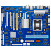
- motherboard
- — [ˈmʌðəbɔːd] —
- материнская плата
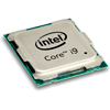
- CPU
- — [siːpiːˈjuː] —
- процессор
Другие варианты перевода: центральный процессор
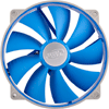
- CPU cooler
- — [siːpiːˈjuː ˈkuːlə] —
- Процессорный кулер
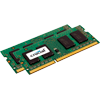
- RAM
- — [ræm] —
- ОЗУ
Другие варианты перевода: оперативная память, память RAM
RAM — Оперативная память (английский: Random Access Memory, RAM.) Память с произвольным доступом или оперативное запоминающее устройство (ОЗУ) — энергозависимая часть системы компьютерной памяти, в которой во время работы компьютера хранится выполняемый машинный код (программы), а также входные, выходные и промежуточные данные, обрабатываемые процессором.

- optical drive
- — [ˈɒptɪk(ə)l drʌɪv] —
- оптический привод
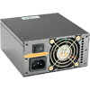
- power supply
- — [ˈpaʊə səˈplʌɪ] —
- блок питания
Другие варианты перевода: источник питания
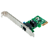
- network card
- — [ˈnɛtwəːk kɑːd] —
- сетевая карта
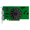
- graphics card
- — [ˈɡrafɪks kɑːd] —
- видеокарта
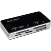
- card reader
- — [kɑːd ˈriːdə] —
- кард-ридер
«RAM» redirects here. For other uses, see Ram.


Random-access memory (RAM; ) is a form of computer memory that can be read and changed in any order, typically used to store working data and machine code.[1][2] A random-access memory device allows data items to be read or written in almost the same amount of time irrespective of the physical location of data inside the memory, in contrast with other direct-access data storage media (such as hard disks, CD-RWs, DVD-RWs and the older magnetic tapes and drum memory), where the time required to read and write data items varies significantly depending on their physical locations on the recording medium, due to mechanical limitations such as media rotation speeds and arm movement.
RAM contains multiplexing and demultiplexing circuitry, to connect the data lines to the addressed storage for reading or writing the entry. Usually more than one bit of storage is accessed by the same address, and RAM devices often have multiple data lines and are said to be «8-bit» or «16-bit», etc. devices.[clarification needed]
In today’s technology, random-access memory takes the form of integrated circuit (IC) chips with MOS (metal–oxide–semiconductor) memory cells. RAM is normally associated with volatile types of memory where stored information is lost if power is removed. The two main types of volatile random-access semiconductor memory are static random-access memory (SRAM) and dynamic random-access memory (DRAM).
Non-volatile RAM has also been developed[3]
and other types of non-volatile memories allow random access for read operations, but either do not allow write operations or have other kinds of limitations on them. These include most types of ROM and a type of flash memory called NOR-Flash.
Use of semiconductor RAM dated back to 1965, when IBM introduced the monolithic (single-chip) 16-bit SP95 SRAM chip for their System/360 Model 95 computer, and Toshiba used discrete DRAM memory cells for its 180-bit Toscal BC-1411 electronic calculator, both based on bipolar transistors. While it offered improved performance over magnetic-core memory, bipolar DRAM could not compete with the lower price of the then-dominant magnetic-core memory.[4]
MOS memory, based on MOS transistors, was developed in the late 1960s, and was the basis for all early commercial semiconductor memory. The first commercial DRAM IC chip, the 1K Intel 1103, was introduced in October 1970.
Synchronous dynamic random-access memory (SDRAM) later debuted with the Samsung KM48SL2000 chip in 1992.
History


Early computers used relays, mechanical counters[5] or delay lines for main memory functions. Ultrasonic delay lines were serial devices which could only reproduce data in the order it was written. Drum memory could be expanded at relatively low cost but efficient retrieval of memory items required knowledge of the physical layout of the drum to optimize speed. Latches built out of vacuum tube triodes, and later, out of discrete transistors, were used for smaller and faster memories such as registers. Such registers were relatively large and too costly to use for large amounts of data; generally only a few dozen or few hundred bits of such memory could be provided.
The first practical form of random-access memory was the Williams tube starting in 1947. It stored data as electrically charged spots on the face of a cathode-ray tube. Since the electron beam of the CRT could read and write the spots on the tube in any order, memory was random access. The capacity of the Williams tube was a few hundred to around a thousand bits, but it was much smaller, faster, and more power-efficient than using individual vacuum tube latches. Developed at the University of Manchester in England, the Williams tube provided the medium on which the first electronically stored program was implemented in the Manchester Baby computer, which first successfully ran a program on 21 June 1948.[6] In fact, rather than the Williams tube memory being designed for the Baby, the Baby was a testbed to demonstrate the reliability of the memory.[7][8]
Magnetic-core memory was invented in 1947 and developed up until the mid-1970s. It became a widespread form of random-access memory, relying on an array of magnetized rings. By changing the sense of each ring’s magnetization, data could be stored with one bit stored per ring. Since every ring had a combination of address wires to select and read or write it, access to any memory location in any sequence was possible. Magnetic core memory was the standard form of computer memory system until displaced by solid-state MOS (metal–oxide–silicon) semiconductor memory in integrated circuits (ICs) during the early 1970s.[9]
Prior to the development of integrated read-only memory (ROM) circuits, permanent (or read-only) random-access memory was often constructed using diode matrices driven by address decoders, or specially wound core rope memory planes.[citation needed]
Semiconductor memory began in the 1960s with bipolar memory, which used bipolar transistors. While it improved performance, it could not compete with the lower price of magnetic core memory.[10]
MOS RAM
The invention of the MOSFET (metal–oxide–semiconductor field-effect transistor), also known as the MOS transistor, by Mohamed M. Atalla and Dawon Kahng at Bell Labs in 1959,[11] led to the development of metal–oxide–semiconductor (MOS) memory by John Schmidt at Fairchild Semiconductor in 1964.[9][12] In addition to higher performance, MOS semiconductor memory was cheaper and consumed less power than magnetic core memory.[9] The development of silicon-gate MOS integrated circuit (MOS IC) technology by Federico Faggin at Fairchild in 1968 enabled the production of MOS memory chips.[13] MOS memory overtook magnetic core memory as the dominant memory technology in the early 1970s.[9]
An integrated bipolar static random-access memory (SRAM) was invented by Robert H. Norman at Fairchild Semiconductor in 1963.[14] It was followed by the development of MOS SRAM by John Schmidt at Fairchild in 1964.[9] SRAM became an alternative to magnetic-core memory, but required six MOS transistors for each bit of data.[15] Commercial use of SRAM began in 1965, when IBM introduced the SP95 memory chip for the System/360 Model 95.[10]
Dynamic random-access memory (DRAM) allowed replacement of a 4 or 6-transistor latch circuit by a single transistor for each memory bit, greatly increasing memory density at the cost of volatility. Data was stored in the tiny capacitance of each transistor, and had to be periodically refreshed every few milliseconds before the charge could leak away. Toshiba’s Toscal BC-1411 electronic calculator, which was introduced in 1965,[16][17][18] used a form of capacitive bipolar DRAM, storing 180-bit data on discrete memory cells, consisting of germanium bipolar transistors and capacitors.[17][18] While it offered improved performance over magnetic-core memory, bipolar DRAM could not compete with the lower price of the then dominant magnetic-core memory.[19]
MOS technology is the basis for modern DRAM. In 1966, Dr. Robert H. Dennard at the IBM Thomas J. Watson Research Center was working on MOS memory. While examining the characteristics of MOS technology, he found it was capable of building capacitors, and that storing a charge or no charge on the MOS capacitor could represent the 1 and 0 of a bit, while the MOS transistor could control writing the charge to the capacitor. This led to his development of a single-transistor DRAM memory cell.[15] In 1967, Dennard filed a patent under IBM for a single-transistor DRAM memory cell, based on MOS technology.[20] The first commercial DRAM IC chip was the Intel 1103, which was manufactured on an 8 µm MOS process with a capacity of 1 kbit, and was released in 1970.[9][21][22]
Synchronous dynamic random-access memory (SDRAM) was developed by Samsung Electronics. The first commercial SDRAM chip was the Samsung KM48SL2000, which had a capacity of 16 Mbit.[23] It was introduced by Samsung in 1992,[24] and mass-produced in 1993.[23] The first commercial DDR SDRAM (double data rate SDRAM) memory chip was Samsung’s 64 Mbit DDR SDRAM chip, released in June 1998.[25] GDDR (graphics DDR) is a form of DDR SGRAM (synchronous graphics RAM), which was first released by Samsung as a 16 Mbit memory chip in 1998.[26]
Types
The two widely used forms of modern RAM are static RAM (SRAM) and dynamic RAM (DRAM). In SRAM, a bit of data is stored using the state of a six-transistor memory cell, typically using six MOSFETs. This form of RAM is more expensive to produce, but is generally faster and requires less dynamic power than DRAM. In modern computers, SRAM is often used as cache memory for the CPU. DRAM stores a bit of data using a transistor and capacitor pair (typically a MOSFET and MOS capacitor, respectively),[27] which together comprise a DRAM cell. The capacitor holds a high or low charge (1 or 0, respectively), and the transistor acts as a switch that lets the control circuitry on the chip read the capacitor’s state of charge or change it. As this form of memory is less expensive to produce than static RAM, it is the predominant form of computer memory used in modern computers.
Both static and dynamic RAM are considered volatile, as their state is lost or reset when power is removed from the system. By contrast, read-only memory (ROM) stores data by permanently enabling or disabling selected transistors, such that the memory cannot be altered. Writeable variants of ROM (such as EEPROM and NOR flash) share properties of both ROM and RAM, enabling data to persist without power and to be updated without requiring special equipment. ECC memory (which can be either SRAM or DRAM) includes special circuitry to detect and/or correct random faults (memory errors) in the stored data, using parity bits or error correction codes.
In general, the term RAM refers solely to solid-state memory devices (either DRAM or SRAM), and more specifically the main memory in most computers. In optical storage, the term DVD-RAM is somewhat of a misnomer since, unlike CD-RW or DVD-RW it does not need to be erased before reuse. Nevertheless, a DVD-RAM behaves much like a hard disc drive if somewhat slower.
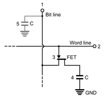
Memory cell
The memory cell is the fundamental building block of computer memory. The memory cell is an electronic circuit that stores one bit of binary information and it must be set to store a logic 1 (high voltage level) and reset to store a logic 0 (low voltage level). Its value is maintained/stored until it is changed by the set/reset process. The value in the memory cell can be accessed by reading it.
In SRAM, the memory cell is a type of flip-flop circuit, usually implemented using FETs. This means that SRAM requires very low power when not being accessed, but it is expensive and has low storage density.
A second type, DRAM, is based around a capacitor. Charging and discharging this capacitor can store a «1» or a «0» in the cell. However, the charge in this capacitor slowly leaks away, and must be refreshed periodically. Because of this refresh process, DRAM uses more power, but it can achieve greater storage densities and lower unit costs compared to SRAM.
|
SRAM Cell (6 Transistors) |
DRAM Cell (1 Transistor and one capacitor) |
Addressing
To be useful, memory cells must be readable and writeable. Within the RAM device, multiplexing and demultiplexing circuitry is used to select memory cells. Typically, a RAM device has a set of address lines A0… An, and for each combination of bits that may be applied to these lines, a set of memory cells are activated. Due to this addressing, RAM devices virtually always have a memory capacity that is a power of two.
Usually several memory cells share the same address. For example, a 4 bit ‘wide’ RAM chip has 4 memory cells for each address. Often the width of the memory and that of the microprocessor are different, for a 32 bit microprocessor, eight 4 bit RAM chips would be needed.
Often more addresses are needed than can be provided by a device. In that case, external multiplexors to the device are used to activate the correct device that is being accessed.
Memory hierarchy
One can read and over-write data in RAM. Many computer systems have a memory hierarchy consisting of processor registers, on-die SRAM caches, external caches, DRAM, paging systems and virtual memory or swap space on a hard drive. This entire pool of memory may be referred to as «RAM» by many developers, even though the various subsystems can have very different access times, violating the original concept behind the random access term in RAM. Even within a hierarchy level such as DRAM, the specific row, column, bank, rank, channel, or interleave organization of the components make the access time variable, although not to the extent that access time to rotating storage media or a tape is variable. The overall goal of using a memory hierarchy is to obtain the highest possible average access performance while minimizing the total cost of the entire memory system (generally, the memory hierarchy follows the access time with the fast CPU registers at the top and the slow hard drive at the bottom).
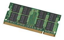
In many modern personal computers, the RAM comes in an easily upgraded form of modules called memory modules or DRAM modules about the size of a few sticks of chewing gum. These can quickly be replaced should they become damaged or when changing needs demand more storage capacity. As suggested above, smaller amounts of RAM (mostly SRAM) are also integrated in the CPU and other ICs on the motherboard, as well as in hard-drives, CD-ROMs, and several other parts of the computer system.
Other uses of RAM
In addition to serving as temporary storage and working space for the operating system and applications, RAM is used in numerous other ways.
Virtual memory
Most modern operating systems employ a method of extending RAM capacity, known as «virtual memory». A portion of the computer’s hard drive is set aside for a paging file or a scratch partition, and the combination of physical RAM and the paging file form the system’s total memory. (For example, if a computer has 2 GB (10243 B) of RAM and a 1 GB page file, the operating system has 3 GB total memory available to it.) When the system runs low on physical memory, it can «swap» portions of RAM to the paging file to make room for new data, as well as to read previously swapped information back into RAM. Excessive use of this mechanism results in thrashing and generally hampers overall system performance, mainly because hard drives are far slower than RAM.
RAM disk
Software can «partition» a portion of a computer’s RAM, allowing it to act as a much faster hard drive that is called a RAM disk. A RAM disk loses the stored data when the computer is shut down, unless memory is arranged to have a standby battery source, or changes to the RAM disk are written out to a nonvolatile disk. The RAM disk is reloaded from the physical disk upon RAM disk initialization.
Shadow RAM
Sometimes, the contents of a relatively slow ROM chip are copied to read/write memory to allow for shorter access times. The ROM chip is then disabled while the initialized memory locations are switched in on the same block of addresses (often write-protected). This process, sometimes called shadowing, is fairly common in both computers and embedded systems.
As a common example, the BIOS in typical personal computers often has an option called «use shadow BIOS» or similar. When enabled, functions that rely on data from the BIOS’s ROM instead use DRAM locations (most can also toggle shadowing of video card ROM or other ROM sections). Depending on the system, this may not result in increased performance, and may cause incompatibilities. For example, some hardware may be inaccessible to the operating system if shadow RAM is used. On some systems the benefit may be hypothetical because the BIOS is not used after booting in favor of direct hardware access. Free memory is reduced by the size of the shadowed ROMs.[28]
Recent developments
Several new types of non-volatile RAM, which preserve data while powered down, are under development. The technologies used include carbon nanotubes and approaches utilizing Tunnel magnetoresistance. Amongst the 1st generation MRAM, a 128 kbit (128 × 210 bytes) chip was manufactured with 0.18 µm technology in the summer of 2003.[citation needed] In June 2004, Infineon Technologies unveiled a 16 MB (16 × 220 bytes) prototype again based on 0.18 µm technology. There are two 2nd generation techniques currently in development: thermal-assisted switching (TAS)[29] which is being developed by Crocus Technology, and spin-transfer torque (STT) on which Crocus, Hynix, IBM, and several other companies are working.[30] Nantero built a functioning carbon nanotube memory prototype 10 GB (10 × 230 bytes) array in 2004. Whether some of these technologies can eventually take significant market share from either DRAM, SRAM, or flash-memory technology, however, remains to be seen.
Since 2006, «solid-state drives» (based on flash memory) with capacities exceeding 256 gigabytes and performance far exceeding traditional disks have become available. This development has started to blur the definition between traditional random-access memory and «disks», dramatically reducing the difference in performance.
Some kinds of random-access memory, such as «EcoRAM», are specifically designed for server farms, where low power consumption is more important than speed.[31]
Memory wall
The «memory wall» is the growing disparity of speed between CPU and memory outside the CPU chip. An important reason for this disparity is the limited communication bandwidth beyond chip boundaries, which is also referred to as bandwidth wall. From 1986 to 2000, CPU speed improved at an annual rate of 55% while memory speed only improved at 10%. Given these trends, it was expected that memory latency would become an overwhelming bottleneck in computer performance.[32]
CPU speed improvements slowed significantly partly due to major physical barriers and partly because current CPU designs have already hit the memory wall in some sense. Intel summarized these causes in a 2005 document.[33]
First of all, as chip geometries shrink and clock frequencies rise, the transistor leakage current increases, leading to excess power consumption and heat… Secondly, the advantages of higher clock speeds are in part negated by memory latency, since memory access times have not been able to keep pace with increasing clock frequencies. Third, for certain applications, traditional serial architectures are becoming less efficient as processors get faster (due to the so-called Von Neumann bottleneck), further undercutting any gains that frequency increases might otherwise buy. In addition, partly due to limitations in the means of producing inductance within solid state devices, resistance-capacitance (RC) delays in signal transmission are growing as feature sizes shrink, imposing an additional bottleneck that frequency increases don’t address.
The RC delays in signal transmission were also noted in «Clock Rate versus IPC: The End of the Road for Conventional Microarchitectures»[34] which projected a maximum of 12.5% average annual CPU performance improvement between 2000 and 2014.
A different concept is the processor-memory performance gap, which can be addressed by 3D integrated circuits that reduce the distance between the logic and memory aspects that are further apart in a 2D chip.[35] Memory subsystem design requires a focus on the gap, which is widening over time.[36] The main method of bridging the gap is the use of caches; small amounts of high-speed memory that houses recent operations and instructions nearby the processor, speeding up the execution of those operations or instructions in cases where they are called upon frequently. Multiple levels of caching have been developed to deal with the widening gap, and the performance of high-speed modern computers relies on evolving caching techniques.[37] There can be up to a 53% difference between the growth in speed of processor and the lagging speed of main memory access.[38]
Solid-state hard drives have continued to increase in speed, from ~400 Mbit/s via SATA3 in 2012 up to ~3 GB/s via NVMe/PCIe in 2018, closing the gap between RAM and hard disk speeds, although RAM continues to be an order of magnitude faster, with single-lane DDR4 3200 capable of 25 GB/s, and modern GDDR even faster. Fast, cheap, non-volatile solid state drives have replaced some functions formerly performed by RAM, such as holding certain data for immediate availability in server farms — 1 terabyte of SSD storage can be had for $200, while 1 TB of RAM would cost thousands of dollars.[39][40]
Timeline
SRAM
| Date of introduction | Chip name | Capacity (bits) | Access time | SRAM type | Manufacturer(s) | Process | MOSFET | Ref |
|---|---|---|---|---|---|---|---|---|
| March 1963 | — | 1-bit | ? | Bipolar (cell) | Fairchild | — | — | [10] |
| 1965 | ? | 8-bit | ? | Bipolar | IBM | ? | — | |
| SP95 | 16-bit | ? | Bipolar | IBM | ? | — | [41] | |
| ? | 64-bit | ? | MOSFET | Fairchild | ? | PMOS | [42] | |
| 1966 | TMC3162 | 16-bit | ? | Bipolar (TTL) | Transitron | ? | — | [9] |
| ? | ? | ? | MOSFET | NEC | ? | ? | [43] | |
| 1968 | ? | 64-bit | ? | MOSFET | Fairchild | ? | PMOS | [43] |
| 144-bit | ? | MOSFET | NEC | ? | NMOS | |||
| 512-bit | ? | MOSFET | IBM | ? | NMOS | [42] | ||
| 1969 | ? | 128-bit | ? | Bipolar | IBM | ? | — | [10] |
| 1101 | 256-bit | 850 ns | MOSFET | Intel | 12,000 nm | PMOS | [44][45][46][47] | |
| 1972 | 2102 | 1 kbit | ? | MOSFET | Intel | ? | NMOS | [44] |
| 1974 | 5101 | 1 kbit | 800 ns | MOSFET | Intel | ? | CMOS | [44][48] |
| 2102A | 1 kbit | 350 ns | MOSFET | Intel | ? | NMOS (depletion) | [44][49] | |
| 1975 | 2114 | 4 kbit | 450 ns | MOSFET | Intel | ? | NMOS | [44][48] |
| 1976 | 2115 | 1 kbit | 70 ns | MOSFET | Intel | ? | NMOS (HMOS) | [44][45] |
| 2147 | 4 kbit | 55 ns | MOSFET | Intel | ? | NMOS (HMOS) | [44][50] | |
| 1977 | ? | 4 kbit | ? | MOSFET | Toshiba | ? | CMOS | [45] |
| 1978 | HM6147 | 4 kbit | 55 ns | MOSFET | Hitachi | 3,000 nm | CMOS (twin-well) | [50] |
| TMS4016 | 16 kbit | ? | MOSFET | Texas Instruments | ? | NMOS | [45] | |
| 1980 | ? | 16 kbit | ? | MOSFET | Hitachi, Toshiba | ? | CMOS | [51] |
| 64 kbit | ? | MOSFET | Matsushita | |||||
| 1981 | ? | 16 kbit | ? | MOSFET | Texas Instruments | 2,500 nm | NMOS | [51] |
| October 1981 | ? | 4 kbit | 18 ns | MOSFET | Matsushita, Toshiba | 2,000 nm | CMOS | [52] |
| 1982 | ? | 64 kbit | ? | MOSFET | Intel | 1,500 nm | NMOS (HMOS) | [51] |
| February 1983 | ? | 64 kbit | 50 ns | MOSFET | Mitsubishi | ? | CMOS | [53] |
| 1984 | ? | 256 kbit | ? | MOSFET | Toshiba | 1,200 nm | CMOS | [51][46] |
| 1987 | ? | 1 Mbit | ? | MOSFET | Sony, Hitachi, Mitsubishi, Toshiba | ? | CMOS | [51] |
| December 1987 | ? | 256 kbit | 10 ns | BiMOS | Texas Instruments | 800 nm | BiCMOS | [54] |
| 1990 | ? | 4 Mbit | 15–23 ns | MOSFET | NEC, Toshiba, Hitachi, Mitsubishi | ? | CMOS | [51] |
| 1992 | ? | 16 Mbit | 12–15 ns | MOSFET | Fujitsu, NEC | 400 nm | ||
| December 1994 | ? | 512 kbit | 2.5 ns | MOSFET | IBM | ? | CMOS (SOI) | [55] |
| 1995 | ? | 4 Mbit | 6 ns | Cache (SyncBurst) | Hitachi | 100 nm | CMOS | [56] |
| 256 Mbit | ? | MOSFET | Hyundai | ? | CMOS | [57] |
DRAM
| Date of introduction | Chip name | Capacity (bits) | DRAM type | Manufacturer(s) | Process | MOSFET | Area | Ref |
|---|---|---|---|---|---|---|---|---|
| 1965 | — | 1 bit | DRAM (cell) | Toshiba | — | — | — | [17][18] |
| 1967 | — | 1 bit | DRAM (cell) | IBM | — | MOS | — | [20][43] |
| 1968 | ? | 256 bit | DRAM (IC) | Fairchild | ? | PMOS | ? | [9] |
| 1969 | — | 1 bit | DRAM (cell) | Intel | — | PMOS | — | [43] |
| 1970 | 1102 | 1 kbit | DRAM (IC) | Intel, Honeywell | ? | PMOS | ? | [43] |
| 1103 | 1 kbit | DRAM | Intel | 8,000 nm | PMOS | 10 mm² | [58][59][21] | |
| 1971 | μPD403 | 1 kbit | DRAM | NEC | ? | NMOS | ? | [60] |
| ? | 2 kbit | DRAM | General Instrument | ? | PMOS | 13 mm² | [61] | |
| 1972 | 2107 | 4 kbit | DRAM | Intel | ? | NMOS | ? | [44][62] |
| 1973 | ? | 8 kbit | DRAM | IBM | ? | PMOS | 19 mm² | [61] |
| 1975 | 2116 | 16 kbit | DRAM | Intel | ? | NMOS | ? | [63][9] |
| 1977 | ? | 64 kbit | DRAM | NTT | ? | NMOS | 35 mm² | [61] |
| 1979 | MK4816 | 16 kbit | PSRAM | Mostek | ? | NMOS | ? | [64] |
| ? | 64 kbit | DRAM | Siemens | ? | VMOS | 25 mm² | [61] | |
| 1980 | ? | 256 kbit | DRAM | NEC, NTT | 1,000–1,500 nm | NMOS | 34–42 mm² | [61] |
| 1981 | ? | 288 kbit | DRAM | IBM | ? | MOS | 25 mm² | [65] |
| 1983 | ? | 64 kbit | DRAM | Intel | 1,500 nm | CMOS | 20 mm² | [61] |
| 256 kbit | DRAM | NTT | ? | CMOS | 31 mm² | |||
| January 5, 1984 | ? | 8 Mbit | DRAM | Hitachi | ? | MOS | ? | [66][67] |
| February 1984 | ? | 1 Mbit | DRAM | Hitachi, NEC | 1,000 nm | NMOS | 74–76 mm² | [61][68] |
| NTT | 800 nm | CMOS | 53 mm² | [61][68] | ||||
| 1984 | TMS4161 | 64 kbit | DPRAM (VRAM) | Texas Instruments | ? | NMOS | ? | [69][70] |
| January 1985 | μPD41264 | 256 kbit | DPRAM (VRAM) | NEC | ? | NMOS | ? | [71][72] |
| June 1986 | ? | 1 Mbit | PSRAM | Toshiba | ? | CMOS | ? | [73] |
| 1986 | ? | 4 Mbit | DRAM | NEC | 800 nm | NMOS | 99 mm² | [61] |
| Texas Instruments, Toshiba | 1,000 nm | CMOS | 100–137 mm² | |||||
| 1987 | ? | 16 Mbit | DRAM | NTT | 700 nm | CMOS | 148 mm² | [61] |
| October 1988 | ? | 512 kbit | HSDRAM | IBM | 1,000 nm | CMOS | 78 mm² | [74] |
| 1991 | ? | 64 Mbit | DRAM | Matsushita, Mitsubishi, Fujitsu, Toshiba | 400 nm | CMOS | ? | [51] |
| 1993 | ? | 256 Mbit | DRAM | Hitachi, NEC | 250 nm | CMOS | ? | |
| 1995 | ? | 4 Mbit | DPRAM (VRAM) | Hitachi | ? | CMOS | ? | [56] |
| January 9, 1995 | ? | 1 Gbit | DRAM | NEC | 250 nm | CMOS | ? | [75][56] |
| Hitachi | 160 nm | CMOS | ? | |||||
| 1996 | ? | 4 Mbit | FRAM | Samsung | ? | NMOS | ? | [76] |
| 1997 | ? | 4 Gbit | QLC | NEC | 150 nm | CMOS | ? | [51] |
| 1998 | ? | 4 Gbit | DRAM | Hyundai | ? | CMOS | ? | [57] |
| June 2001 | TC51W3216XB | 32 Mbit | PSRAM | Toshiba | ? | CMOS | ? | [77] |
| February 2001 | ? | 4 Gbit | DRAM | Samsung | 100 nm | CMOS | ? | [51][78] |
SDRAM
| Date of introduction | Chip name | Capacity (bits)[79] | SDRAM type | Manufacturer(s) | Process | MOSFET | Area | Ref |
|---|---|---|---|---|---|---|---|---|
| 1992 | KM48SL2000 | 16 Mbit | SDR | Samsung | ? | CMOS | ? | [80][23] |
| 1996 | MSM5718C50 | 18 Mbit | RDRAM | Oki | ? | CMOS | 325 mm2 | [81] |
| N64 RDRAM | 36 Mbit | RDRAM | NEC | ? | CMOS | ? | [82] | |
| ? | 1024 Mbit | SDR | Mitsubishi | 150 nm | CMOS | ? | [51] | |
| 1997 | ? | 1024 Mbit | SDR | Hyundai | ? | SOI | ? | [57] |
| 1998 | MD5764802 | 64 Mbit | RDRAM | Oki | ? | CMOS | 325 mm2 | [81] |
| March 1998 | Direct RDRAM | 72 Mbit | RDRAM | Rambus | ? | CMOS | ? | [83] |
| June 1998 | ? | 64 Mbit | DDR | Samsung | ? | CMOS | ? | [84][85][86] |
| 1998 | ? | 64 Mbit | DDR | Hyundai | ? | CMOS | ? | [57] |
| 128 Mbit | SDR | Samsung | ? | CMOS | ? | [87][85] | ||
| 1999 | ? | 128 Mbit | DDR | Samsung | ? | CMOS | ? | [85] |
| 1024 Mbit | DDR | Samsung | 140 nm | CMOS | ? | [51] | ||
| 2000 | GS eDRAM | 32 Mbit | eDRAM | Sony, Toshiba | 180 nm | CMOS | 279 mm2 | [88] |
| 2001 | ? | 288 Mbit | RDRAM | Hynix | ? | CMOS | ? | [89] |
| ? | DDR2 | Samsung | 100 nm | CMOS | ? | [86][51] | ||
| 2002 | ? | 256 Mbit | SDR | Hynix | ? | CMOS | ? | [89] |
| 2003 | EE+GS eDRAM | 32 Mbit | eDRAM | Sony, Toshiba | 90 nm | CMOS | 86 mm2 | [88] |
| ? | 72 Mbit | DDR3 | Samsung | 90 nm | CMOS | ? | [90] | |
| 512 Mbit | DDR2 | Hynix | ? | CMOS | ? | [89] | ||
| Elpida | 110 nm | CMOS | ? | [91] | ||||
| 1024 Mbit | DDR2 | Hynix | ? | CMOS | ? | [89] | ||
| 2004 | ? | 2048 Mbit | DDR2 | Samsung | 80 nm | CMOS | ? | [92] |
| 2005 | EE+GS eDRAM | 32 Mbit | eDRAM | Sony, Toshiba | 65 nm | CMOS | 86 mm2 | [93] |
| Xenos eDRAM | 80 Mbit | eDRAM | NEC | 90 nm | CMOS | ? | [94] | |
| ? | 512 Mbit | DDR3 | Samsung | 80 nm | CMOS | ? | [86][95] | |
| 2006 | ? | 1024 Mbit | DDR2 | Hynix | 60 nm | CMOS | ? | [89] |
| 2008 | ? | ? | LPDDR2 | Hynix | ? | |||
| April 2008 | ? | 8192 Mbit | DDR3 | Samsung | 50 nm | CMOS | ? | [96] |
| 2008 | ? | 16384 Mbit | DDR3 | Samsung | 50 nm | CMOS | ? | |
| 2009 | ? | ? | DDR3 | Hynix | 44 nm | CMOS | ? | [89] |
| 2048 Mbit | DDR3 | Hynix | 40 nm | |||||
| 2011 | ? | 16384 Mbit | DDR3 | Hynix | 40 nm | CMOS | ? | [97] |
| 2048 Mbit | DDR4 | Hynix | 30 nm | CMOS | ? | [97] | ||
| 2013 | ? | ? | LPDDR4 | Samsung | 20 nm | CMOS | ? | [97] |
| 2014 | ? | 8192 Mbit | LPDDR4 | Samsung | 20 nm | CMOS | ? | [98] |
| 2015 | ? | 12 Gbit | LPDDR4 | Samsung | 20 nm | CMOS | ? | [87] |
| 2018 | ? | 8192 Mbit | LPDDR5 | Samsung | 10 nm | FinFET | ? | [99] |
| 128 Gbit | DDR4 | Samsung | 10 nm | FinFET | ? | [100] |
SGRAM and HBM
| Date of introduction | Chip name | Capacity (bits)[79] | SDRAM type | Manufacturer(s) | Process | MOSFET | Area | Ref |
|---|---|---|---|---|---|---|---|---|
| November 1994 | HM5283206 | 8 Mbit | SGRAM (SDR) | Hitachi | 350 nm | CMOS | 58 mm2 | [101][102] |
| December 1994 | μPD481850 | 8 Mbit | SGRAM (SDR) | NEC | ? | CMOS | 280 mm2 | [103][104] |
| 1997 | μPD4811650 | 16 Mbit | SGRAM (SDR) | NEC | 350 nm | CMOS | 280 mm2 | [105][106] |
| September 1998 | ? | 16 Mbit | SGRAM (GDDR) | Samsung | ? | CMOS | ? | [84] |
| 1999 | KM4132G112 | 32 Mbit | SGRAM (SDR) | Samsung | ? | CMOS | ? | [107] |
| 2002 | ? | 128 Mbit | SGRAM (GDDR2) | Samsung | ? | CMOS | ? | [108] |
| 2003 | ? | 256 Mbit | SGRAM (GDDR2) | Samsung | ? | CMOS | ? | [108] |
| SGRAM (GDDR3) | ||||||||
| March 2005 | K4D553238F | 256 Mbit | SGRAM (GDDR) | Samsung | ? | CMOS | 77 mm2 | [109] |
| October 2005 | ? | 256 Mbit | SGRAM (GDDR4) | Samsung | ? | CMOS | ? | [110] |
| 2005 | ? | 512 Mbit | SGRAM (GDDR4) | Hynix | ? | CMOS | ? | [89] |
| 2007 | ? | 1024 Mbit | SGRAM (GDDR5) | Hynix | 60 nm | |||
| 2009 | ? | 2048 Mbit | SGRAM (GDDR5) | Hynix | 40 nm | |||
| 2010 | K4W1G1646G | 1024 Mbit | SGRAM (GDDR3) | Samsung | ? | CMOS | 100 mm2 | [111] |
| 2012 | ? | 4096 Mbit | SGRAM (GDDR3) | SK Hynix | ? | CMOS | ? | [97] |
| 2013 | ? | ? | HBM | |||||
| March 2016 | MT58K256M32JA | 8 Gbit | SGRAM (GDDR5X) | Micron | 20 nm | CMOS | 140 mm2 | [112] |
| June 2016 | ? | 32 Gbit | HBM2 | Samsung | 20 nm | CMOS | ? | [113][114] |
| 2017 | ? | 64 Gbit | HBM2 | Samsung | 20 nm | CMOS | ? | [113] |
| January 2018 | K4ZAF325BM | 16 Gbit | SGRAM (GDDR6) | Samsung | 10 nm | FinFET | 225 mm2 | [115][116][117] |
See also
- CAS latency (CL)
- Hybrid Memory Cube
- Multi-channel memory architecture
- Registered/buffered memory
- RAM parity
- Memory Interconnect/RAM buses
- Memory geometry
- Chip creep
- Read-mostly memory (RMM)
- Electrochemical random-access memory
References
- ^ «RAM». Cambridge English Dictionary. Retrieved 11 July 2019.
- ^ «RAM». Oxford Advanced Learner’s Dictionary. Retrieved 11 July 2019.
- ^ Gallagher, Sean (April 4, 2013). «Memory that never forgets: non-volatile DIMMs hit the market». Ars Technica. Archived from the original on July 8, 2017.
- ^ «1966: Semiconductor RAMs Serve High-speed Storage Needs». Computer History Museum.
- ^ «IBM Archives — FAQ’s for Products and Services». ibm.com. Archived from the original on 2012-10-23.
- ^ Napper, Brian, Computer 50: The University of Manchester Celebrates the Birth of the Modern Computer, archived from the original on 4 May 2012, retrieved 26 May 2012
- ^ Williams, F. C.; Kilburn, T. (Sep 1948), «Electronic Digital Computers», Nature, 162 (4117): 487, Bibcode:1948Natur.162..487W, doi:10.1038/162487a0, S2CID 4110351. Reprinted in The Origins of Digital Computers.
- ^ Williams, F. C.; Kilburn, T.; Tootill, G. C. (Feb 1951), «Universal High-Speed Digital Computers: A Small-Scale Experimental Machine», Proc. IEE, 98 (61): 13–28, doi:10.1049/pi-2.1951.0004, archived from the original on 2013-11-17.
- ^ a b c d e f g h i «1970: Semiconductors compete with magnetic cores». Computer History Museum. Retrieved 19 June 2019.
- ^ a b c d «1966: Semiconductor RAMs Serve High-speed Storage Needs». Computer History Museum. Retrieved 19 June 2019.
- ^ «1960 – Metal Oxide Semiconductor (MOS) Transistor Demonstrated». The Silicon Engine. Computer History Museum.
- ^ Solid State Design – Vol. 6. Horizon House. 1965.
- ^ «1968: Silicon Gate Technology Developed for ICs». Computer History Museum. Retrieved 10 August 2019.
- ^ US patent 3562721, Robert H. Norman, «Solid State Switching and Memory Apparatus», published 9 February1971
- ^ a b «DRAM». IBM100. IBM. 9 August 2017. Retrieved 20 September 2019.
- ^ Toscal BC-1411 calculator. Archived 2017-07-29 at the Wayback Machine, Science Museum, London.
- ^ a b c «Spec Sheet for Toshiba «TOSCAL» BC-1411″. Old Calculator Web Museum. Archived from the original on 3 July 2017. Retrieved 8 May 2018.
- ^ a b c Toshiba «Toscal» BC-1411 Desktop Calculator Archived 2007-05-20 at the Wayback Machine
- ^ «1966: Semiconductor RAMs Serve High-speed Storage Needs». Computer History Museum.
- ^ a b «Robert Dennard». Encyclopedia Britannica. Retrieved 8 July 2019.
- ^ a b Lojek, Bo (2007). History of Semiconductor Engineering. Springer Science & Business Media. pp. 362–363. ISBN 9783540342588.
The i1103 was manufactured on a 6-mask silicon-gate P-MOS process with 8 μm minimum features. The resulting product had a 2,400 µm² memory cell size, a die size just under 10 mm², and sold for around $21.
- ^ Bellis, Mary. «The Invention of the Intel 1103».
- ^ a b c «Electronic Design». Electronic Design. Hayden Publishing Company. 41 (15–21). 1993.
The first commercial synchronous DRAM, the Samsung 16-Mbit KM48SL2000, employs a single-bank architecture that lets system designers easily transition from asynchronous to synchronous systems.
- ^ «KM48SL2000-7 Datasheet». Samsung. August 1992. Retrieved 19 June 2019.
- ^ «Samsung Electronics Develops First 128Mb SDRAM with DDR/SDR Manufacturing Option». Samsung Electronics. Samsung. 10 February 1999. Retrieved 23 June 2019.
- ^ «Samsung Electronics Comes Out with Super-Fast 16M DDR SGRAMs». Samsung Electronics. Samsung. 17 September 1998. Retrieved 23 June 2019.
- ^ Sze, Simon M. (2002). Semiconductor Devices: Physics and Technology (PDF) (2nd ed.). Wiley. p. 214. ISBN 0-471-33372-7.
- ^ «Shadow Ram». Archived from the original on 2006-10-29. Retrieved 2007-07-24.
- ^ The Emergence of Practical MRAM «Crocus Technology | Magnetic Sensors | TMR Sensors» (PDF). Archived from the original (PDF) on 2011-04-27. Retrieved 2009-07-20.
- ^ «Tower invests in Crocus, tips MRAM foundry deal». EETimes. Archived from the original on 2012-01-19.
- ^
«EcoRAM held up as less power-hungry option than DRAM for server farms» Archived 2008-06-30 at the Wayback Machine
by Heather Clancy 2008 - ^ The term was coined in «Archived copy» (PDF). Archived (PDF) from the original on 2012-04-06. Retrieved 2011-12-14.
{{cite web}}: CS1 maint: archived copy as title (link). - ^ «Platform 2015: Intel® Processor and Platform Evolution for the Next Decade» (PDF). March 2, 2005. Archived (PDF) from the original on April 27, 2011.
- ^ Agarwal, Vikas; Hrishikesh, M. S.; Keckler, Stephen W.; Burger, Doug (June 10–14, 2000). «Clock Rate versus IPC: The End of the Road for Conventional Microarchitectures» (PDF). Proceedings of the 27th Annual International Symposium on Computer Architecture. 27th Annual International Symposium on Computer Architecture. Vancouver, BC. Retrieved 14 July 2018.
- ^ Rainer Waser (2012). Nanoelectronics and Information Technology. John Wiley & Sons. p. 790. ISBN 9783527409273. Archived from the original on August 1, 2016. Retrieved March 31, 2014.
- ^ Chris Jesshope and Colin Egan (2006). Advances in Computer Systems Architecture: 11th Asia-Pacific Conference, ACSAC 2006, Shanghai, China, September 6-8, 2006, Proceedings. Springer. p. 109. ISBN 9783540400561. Archived from the original on August 1, 2016. Retrieved March 31, 2014.
- ^ Ahmed Amine Jerraya and Wayne Wolf (2005). Multiprocessor Systems-on-chips. Morgan Kaufmann. pp. 90–91. ISBN 9780123852519. Archived from the original on August 1, 2016. Retrieved March 31, 2014.
- ^ Celso C. Ribeiro and Simone L. Martins (2004). Experimental and Efficient Algorithms: Third International Workshop, WEA 2004, Angra Dos Reis, Brazil, May 25-28, 2004, Proceedings, Volume 3. Springer. p. 529. ISBN 9783540220671. Archived from the original on August 1, 2016. Retrieved March 31, 2014.
- ^ «SSD Prices Continue to Fall, Now Upgrade Your Hard Drive!». MiniTool. 2018-09-03. Retrieved 2019-03-28.
- ^ Coppock, Mark (31 January 2017). «If you’re buying or upgrading your PC, expect to pay more for RAM». www.digitaltrends.com. Retrieved 2019-03-28.
- ^ IBM first in IC memory. Computer History Museum. IBM Corporation. 1965. Retrieved 19 June 2019.
- ^ a b Sah, Chih-Tang (October 1988). «Evolution of the MOS transistor-from conception to VLSI» (PDF). Proceedings of the IEEE. 76 (10): 1280–1326 (1303). Bibcode:1988IEEEP..76.1280S. doi:10.1109/5.16328. ISSN 0018-9219.
- ^ a b c d e «Late 1960s: Beginnings of MOS memory» (PDF). Semiconductor History Museum of Japan. 2019-01-23. Retrieved 27 June 2019.
- ^ a b c d e f g h «A chronological list of Intel products. The products are sorted by date» (PDF). Intel museum. Intel Corporation. July 2005. Archived from the original (PDF) on August 9, 2007. Retrieved July 31, 2007.
- ^ a b c d «1970s: SRAM evolution» (PDF). Semiconductor History Museum of Japan. Retrieved 27 June 2019.
- ^ a b Pimbley, J. (2012). Advanced CMOS Process Technology. Elsevier. p. 7. ISBN 9780323156806.
- ^ «Intel Memory». Intel Vintage. Retrieved 2019-07-06.
- ^ a b Component Data Catalog (PDF). Intel. 1978. p. 3. Retrieved 27 June 2019.
- ^ «Silicon Gate MOS 2102A». Intel. Retrieved 27 June 2019.
- ^ a b «1978: Double-well fast CMOS SRAM (Hitachi)» (PDF). Semiconductor History Museum of Japan. Retrieved 5 July 2019.
- ^ a b c d e f g h i j k l «Memory». STOL (Semiconductor Technology Online). Retrieved 25 June 2019.
- ^ Isobe, Mitsuo; Uchida, Yukimasa; Maeguchi, Kenji; Mochizuki, T.; Kimura, M.; Hatano, H.; Mizutani, Y.; Tango, H. (October 1981). «An 18 ns CMOS/SOS 4K static RAM». IEEE Journal of Solid-State Circuits. 16 (5): 460–465. Bibcode:1981IJSSC..16..460I. doi:10.1109/JSSC.1981.1051623. S2CID 12992820.
- ^ Yoshimoto, M.; Anami, K.; Shinohara, H.; Yoshihara, T.; Takagi, H.; Nagao, S.; Kayano, S.; Nakano, T. (1983). «A 64Kb full CMOS RAM with divided word line structure». 1983 IEEE International Solid-State Circuits Conference. Digest of Technical Papers. XXVI: 58–59. doi:10.1109/ISSCC.1983.1156503. S2CID 34837669.
- ^ Havemann, Robert H.; Eklund, R. E.; Tran, Hiep V.; Haken, R. A.; Scott, D. B.; Fung, P. K.; Ham, T. E.; Favreau, D. P.; Virkus, R. L. (December 1987). «An 0.8 #181;m 256K BiCMOS SRAM technology». 1987 International Electron Devices Meeting: 841–843. doi:10.1109/IEDM.1987.191564. S2CID 40375699.
- ^ Shahidi, Ghavam G.; Davari, Bijan; Dennard, Robert H.; Anderson, C. A.; Chappell, B. A.; et al. (December 1994). «A room temperature 0.1 µm CMOS on SOI». IEEE Transactions on Electron Devices. 41 (12): 2405–2412. Bibcode:1994ITED…41.2405S. doi:10.1109/16.337456. S2CID 108832941.
- ^ a b c «Japanese Company Profiles» (PDF). Smithsonian Institution. 1996. Retrieved 27 June 2019.
- ^ a b c d «History: 1990s». SK Hynix. Archived from the original on 5 February 2021. Retrieved 6 July 2019.
- ^ «Intel: 35 Years of Innovation (1968–2003)» (PDF). Intel. 2003. Retrieved 26 June 2019.
- ^ The DRAM memory of Robert Dennard history-computer.com
- ^ «Manufacturers in Japan enter the DRAM market and integration densities are improved» (PDF). Semiconductor History Museum of Japan. Retrieved 27 June 2019.
- ^ a b c d e f g h i j Gealow, Jeffrey Carl (10 August 1990). «Impact of Processing Technology on DRAM Sense Amplifier Design» (PDF). Massachusetts Institute of Technology. pp. 149–166. Retrieved 25 June 2019 – via CORE.
- ^ «Silicon Gate MOS 2107A». Intel. Retrieved 27 June 2019.
- ^ «One of the Most Successful 16K Dynamic RAMs: The 4116». National Museum of American History. Smithsonian Institution. Retrieved 20 June 2019.
- ^ Memory Data Book And Designers Guide (PDF). Mostek. March 1979. pp. 9 & 183.
- ^ «The Cutting Edge of IC Technology: The First 294,912-Bit (288K) Dynamic RAM». National Museum of American History. Smithsonian Institution. Retrieved 20 June 2019.
- ^ «Computer History for 1984». Computer Hope. Retrieved 25 June 2019.
- ^ «Japanese Technical Abstracts». Japanese Technical Abstracts. University Microfilms. 2 (3–4): 161. 1987.
The announcement of 1M DRAM in 1984 began the era of megabytes.
- ^ a b Robinson, Arthur L. (11 May 1984). «Experimental Memory Chips Reach 1 Megabit: As they become larger, memories become an increasingly important part of the integrated circuit business, technologically and economically». Science. 224 (4649): 590–592. doi:10.1126/science.224.4649.590. ISSN 0036-8075. PMID 17838349.
- ^ MOS Memory Data Book (PDF). Texas Instruments. 1984. pp. 4–15. Retrieved 21 June 2019.
- ^ «Famous Graphics Chips: TI TMS34010 and VRAM». IEEE Computer Society. Retrieved 29 June 2019.
- ^ «μPD41264 256K Dual Port Graphics Buffer» (PDF). NEC Electronics. Retrieved 21 June 2019.
- ^ «Sense amplifier circuit for switching plural inputs at low power». Google Patents. Retrieved 21 June 2019.
- ^ «Fine CMOS techniques create 1M VSRAM». Japanese Technical Abstracts. University Microfilms. 2 (3–4): 161. 1987.
- ^ Hanafi, Hussein I.; Lu, Nicky C. C.; Chao, H. H.; Hwang, Wei; Henkels, W. H.; Rajeevakumar, T. V.; Terman, L. M.; Franch, Robert L. (October 1988). «A 20-ns 128-kbit*4 high speed DRAM with 330-Mbit/s data rate». IEEE Journal of Solid-State Circuits. 23 (5): 1140–1149. Bibcode:1988IJSSC..23.1140L. doi:10.1109/4.5936.
- ^ Breaking the gigabit barrier, DRAMs at ISSCC portend major system-design impact. (dynamic random access memory; International Solid-State Circuits Conference; Hitachi Ltd. and NEC Corp. research and development) Highbeam Business, January 9, 1995
- ^ Scott, J.F. (2003). «Nano-Ferroelectrics». In Tsakalakos, Thomas; Ovid’ko, Ilya A.; Vasudevan, Asuri K. (eds.). Nanostructures: Synthesis, Functional Properties and Application. Springer Science & Business Media. pp. 584–600 (597). ISBN 9789400710191.
- ^ «Toshiba’s new 32 Mb Pseudo-SRAM is no fake». The Engineer. 24 June 2001. Retrieved 29 June 2019.
- ^ «A Study of the DRAM industry» (PDF). MIT. 8 June 2010. Retrieved 29 June 2019.
- ^ a b Here, K, M, G, or T refer to the binary prefixes based on powers of 1024.
- ^ «KM48SL2000-7 Datasheet». Samsung. August 1992. Retrieved 19 June 2019.
- ^ a b «MSM5718C50/MD5764802» (PDF). Oki Semiconductor. February 1999. Archived (PDF) from the original on 2019-06-21. Retrieved 21 June 2019.
- ^ «Ultra 64 Tech Specs». Next Generation. No. 14. Imagine Media. February 1996. p. 40.
- ^ «Direct RDRAM» (PDF). Rambus. 12 March 1998. Archived (PDF) from the original on 2019-06-21. Retrieved 21 June 2019.
- ^ a b «Samsung Electronics Comes Out with Super-Fast 16M DDR SGRAMs». Samsung Electronics. Samsung. 17 September 1998. Retrieved 23 June 2019.
- ^ a b c «Samsung Electronics Develops First 128Mb SDRAM with DDR/SDR Manufacturing Option». Samsung Electronics. Samsung. 10 February 1999. Retrieved 23 June 2019.
- ^ a b c «Samsung Demonstrates World’s First DDR 3 Memory Prototype». Phys.org. 17 February 2005. Retrieved 23 June 2019.
- ^ a b «History». Samsung Electronics. Samsung. Retrieved 19 June 2019.
- ^ a b «EMOTION ENGINE AND GRAPHICS SYNTHESIZER USED IN THE CORE OF PLAYSTATION BECOME ONE CHIP» (PDF). Sony. April 21, 2003. Archived (PDF) from the original on 2017-02-27. Retrieved 26 June 2019.
- ^ a b c d e f g «History: 2000s». az5miao. Retrieved 4 April 2022.
{{cite web}}: CS1 maint: url-status (link) - ^ «Samsung Develops the Industry’s Fastest DDR3 SRAM for High Performance EDP and Network Applications». Samsung Semiconductor. Samsung. 29 January 2003. Retrieved 25 June 2019.
- ^ «Elpida ships 2GB DDR2 modules». The Inquirer. 4 November 2003. Archived from the original on July 10, 2019. Retrieved 25 June 2019.
{{cite news}}: CS1 maint: unfit URL (link) - ^ «Samsung Shows Industry’s First 2-Gigabit DDR2 SDRAM». Samsung Semiconductor. Samsung. 20 September 2004. Retrieved 25 June 2019.
- ^ «ソニー、65nm対応の半導体設備を導入。3年間で2,000億円の投資». pc.watch.impress.co.jp. Archived from the original on 2016-08-13.
- ^ ATI engineers by way of Beyond 3D’s Dave Baumann
- ^ «Our Proud Heritage from 2000 to 2009». Samsung Semiconductor. Samsung. Retrieved 25 June 2019.
- ^ «Samsung 50nm 2GB DDR3 chips are industry’s smallest». SlashGear. 29 September 2008. Retrieved 25 June 2019.
- ^ a b c d «History: 2010s». az5miao. Retrieved 4 April 2022.
- ^ «Our Proud Heritage from 2010 to Now». Samsung Semiconductor. Samsung. Retrieved 25 June 2019.
- ^ «Samsung Electronics Announces Industry’s First 8Gb LPDDR5 DRAM for 5G and AI-powered Mobile Applications». Samsung. July 17, 2018. Retrieved 8 July 2019.
- ^ «Samsung Unleashes a Roomy DDR4 256GB RAM». Tom’s Hardware. 6 September 2018. Archived from the original on June 21, 2019. Retrieved 4 April 2022.
- ^ HM5283206 Datasheet. Hitachi. 11 November 1994. Retrieved 10 July 2019.
- ^ «Hitachi HM5283206FP10 8Mbit SGRAM» (PDF). Smithsonian Institution. Archived (PDF) from the original on 2003-07-16. Retrieved 10 July 2019.
- ^ μPD481850 Datasheet. NEC. 6 December 1994. Retrieved 10 July 2019.
- ^ NEC Application Specific Memory. NEC. Fall 1995. p. 359. Retrieved 21 June 2019.
- ^ UPD4811650 Datasheet. NEC. December 1997. Retrieved 10 July 2019.
- ^ Takeuchi, Kei (1998). «16M-BIT SYNCHRONOUS GRAPHICS RAM: μPD4811650». NEC Device Technology International (48). Retrieved 10 July 2019.
- ^ «Samsung Announces the World’s First 222 MHz 32Mbit SGRAM for 3D Graphics and Networking Applications». Samsung Semiconductor. Samsung. 12 July 1999. Retrieved 10 July 2019.
- ^ a b «Samsung Electronics Announces JEDEC-Compliant 256Mb GDDR2 for 3D Graphics». Samsung Electronics. Samsung. 28 August 2003. Retrieved 26 June 2019.
- ^ «K4D553238F Datasheet». Samsung Electronics. March 2005. Retrieved 10 July 2019.
- ^ «Samsung Electronics Develops Industry’s First Ultra-Fast GDDR4 Graphics DRAM». Samsung Semiconductor. Samsung. October 26, 2005. Retrieved 8 July 2019.
- ^ «K4W1G1646G-BC08 Datasheet» (PDF). Samsung Electronics. November 2010. Archived (PDF) from the original on 2022-01-24. Retrieved 10 July 2019.
- ^ Shilov, Anton (March 29, 2016). «Micron Begins to Sample GDDR5X Memory, Unveils Specs of Chips». AnandTech. Retrieved 16 July 2019.
- ^ a b Shilov, Anton (July 19, 2017). «Samsung Increases Production Volumes of 8 GB HBM2 Chips Due to Growing Demand». AnandTech. Retrieved 29 June 2019.
- ^ «HBM». Samsung Semiconductor. Samsung. Retrieved 16 July 2019.
- ^ «Samsung Electronics Starts Producing Industry’s First 16-Gigabit GDDR6 for Advanced Graphics Systems». Samsung. January 18, 2018. Retrieved 15 July 2019.
- ^ Killian, Zak (18 January 2018). «Samsung fires up its foundries for mass production of GDDR6 memory». Tech Report. Retrieved 18 January 2018.
- ^ «Samsung Begins Producing The Fastest GDDR6 Memory In The World». Wccftech. 18 January 2018. Retrieved 16 July 2019.
External links
 Media related to RAM at Wikimedia Commons
«RAM» redirects here. For other uses, see Ram.
Random-access memory (RAM; ) is a form of computer memory that can be read and changed in any order, typically used to store working data and machine code.[1][2] A random-access memory device allows data items to be read or written in almost the same amount of time irrespective of the physical location of data inside the memory, in contrast with other direct-access data storage media (such as hard disks, CD-RWs, DVD-RWs and the older magnetic tapes and drum memory), where the time required to read and write data items varies significantly depending on their physical locations on the recording medium, due to mechanical limitations such as media rotation speeds and arm movement.
RAM contains multiplexing and demultiplexing circuitry, to connect the data lines to the addressed storage for reading or writing the entry. Usually more than one bit of storage is accessed by the same address, and RAM devices often have multiple data lines and are said to be «8-bit» or «16-bit», etc. devices.[clarification needed]
In today’s technology, random-access memory takes the form of integrated circuit (IC) chips with MOS (metal–oxide–semiconductor) memory cells. RAM is normally associated with volatile types of memory where stored information is lost if power is removed. The two main types of volatile random-access semiconductor memory are static random-access memory (SRAM) and dynamic random-access memory (DRAM).
Non-volatile RAM has also been developed[3]
and other types of non-volatile memories allow random access for read operations, but either do not allow write operations or have other kinds of limitations on them. These include most types of ROM and a type of flash memory called NOR-Flash.
Use of semiconductor RAM dated back to 1965, when IBM introduced the monolithic (single-chip) 16-bit SP95 SRAM chip for their System/360 Model 95 computer, and Toshiba used discrete DRAM memory cells for its 180-bit Toscal BC-1411 electronic calculator, both based on bipolar transistors. While it offered improved performance over magnetic-core memory, bipolar DRAM could not compete with the lower price of the then-dominant magnetic-core memory.[4]
MOS memory, based on MOS transistors, was developed in the late 1960s, and was the basis for all early commercial semiconductor memory. The first commercial DRAM IC chip, the 1K Intel 1103, was introduced in October 1970.
Synchronous dynamic random-access memory (SDRAM) later debuted with the Samsung KM48SL2000 chip in 1992.
History
Early computers used relays, mechanical counters[5] or delay lines for main memory functions. Ultrasonic delay lines were serial devices which could only reproduce data in the order it was written. Drum memory could be expanded at relatively low cost but efficient retrieval of memory items required knowledge of the physical layout of the drum to optimize speed. Latches built out of vacuum tube triodes, and later, out of discrete transistors, were used for smaller and faster memories such as registers. Such registers were relatively large and too costly to use for large amounts of data; generally only a few dozen or few hundred bits of such memory could be provided.
The first practical form of random-access memory was the Williams tube starting in 1947. It stored data as electrically charged spots on the face of a cathode-ray tube. Since the electron beam of the CRT could read and write the spots on the tube in any order, memory was random access. The capacity of the Williams tube was a few hundred to around a thousand bits, but it was much smaller, faster, and more power-efficient than using individual vacuum tube latches. Developed at the University of Manchester in England, the Williams tube provided the medium on which the first electronically stored program was implemented in the Manchester Baby computer, which first successfully ran a program on 21 June 1948.[6] In fact, rather than the Williams tube memory being designed for the Baby, the Baby was a testbed to demonstrate the reliability of the memory.[7][8]
Magnetic-core memory was invented in 1947 and developed up until the mid-1970s. It became a widespread form of random-access memory, relying on an array of magnetized rings. By changing the sense of each ring’s magnetization, data could be stored with one bit stored per ring. Since every ring had a combination of address wires to select and read or write it, access to any memory location in any sequence was possible. Magnetic core memory was the standard form of computer memory system until displaced by solid-state MOS (metal–oxide–silicon) semiconductor memory in integrated circuits (ICs) during the early 1970s.[9]
Prior to the development of integrated read-only memory (ROM) circuits, permanent (or read-only) random-access memory was often constructed using diode matrices driven by address decoders, or specially wound core rope memory planes.[citation needed]
Semiconductor memory began in the 1960s with bipolar memory, which used bipolar transistors. While it improved performance, it could not compete with the lower price of magnetic core memory.[10]
MOS RAM
The invention of the MOSFET (metal–oxide–semiconductor field-effect transistor), also known as the MOS transistor, by Mohamed M. Atalla and Dawon Kahng at Bell Labs in 1959,[11] led to the development of metal–oxide–semiconductor (MOS) memory by John Schmidt at Fairchild Semiconductor in 1964.[9][12] In addition to higher performance, MOS semiconductor memory was cheaper and consumed less power than magnetic core memory.[9] The development of silicon-gate MOS integrated circuit (MOS IC) technology by Federico Faggin at Fairchild in 1968 enabled the production of MOS memory chips.[13] MOS memory overtook magnetic core memory as the dominant memory technology in the early 1970s.[9]
An integrated bipolar static random-access memory (SRAM) was invented by Robert H. Norman at Fairchild Semiconductor in 1963.[14] It was followed by the development of MOS SRAM by John Schmidt at Fairchild in 1964.[9] SRAM became an alternative to magnetic-core memory, but required six MOS transistors for each bit of data.[15] Commercial use of SRAM began in 1965, when IBM introduced the SP95 memory chip for the System/360 Model 95.[10]
Dynamic random-access memory (DRAM) allowed replacement of a 4 or 6-transistor latch circuit by a single transistor for each memory bit, greatly increasing memory density at the cost of volatility. Data was stored in the tiny capacitance of each transistor, and had to be periodically refreshed every few milliseconds before the charge could leak away. Toshiba’s Toscal BC-1411 electronic calculator, which was introduced in 1965,[16][17][18] used a form of capacitive bipolar DRAM, storing 180-bit data on discrete memory cells, consisting of germanium bipolar transistors and capacitors.[17][18] While it offered improved performance over magnetic-core memory, bipolar DRAM could not compete with the lower price of the then dominant magnetic-core memory.[19]
MOS technology is the basis for modern DRAM. In 1966, Dr. Robert H. Dennard at the IBM Thomas J. Watson Research Center was working on MOS memory. While examining the characteristics of MOS technology, he found it was capable of building capacitors, and that storing a charge or no charge on the MOS capacitor could represent the 1 and 0 of a bit, while the MOS transistor could control writing the charge to the capacitor. This led to his development of a single-transistor DRAM memory cell.[15] In 1967, Dennard filed a patent under IBM for a single-transistor DRAM memory cell, based on MOS technology.[20] The first commercial DRAM IC chip was the Intel 1103, which was manufactured on an 8 µm MOS process with a capacity of 1 kbit, and was released in 1970.[9][21][22]
Synchronous dynamic random-access memory (SDRAM) was developed by Samsung Electronics. The first commercial SDRAM chip was the Samsung KM48SL2000, which had a capacity of 16 Mbit.[23] It was introduced by Samsung in 1992,[24] and mass-produced in 1993.[23] The first commercial DDR SDRAM (double data rate SDRAM) memory chip was Samsung’s 64 Mbit DDR SDRAM chip, released in June 1998.[25] GDDR (graphics DDR) is a form of DDR SGRAM (synchronous graphics RAM), which was first released by Samsung as a 16 Mbit memory chip in 1998.[26]
Types
The two widely used forms of modern RAM are static RAM (SRAM) and dynamic RAM (DRAM). In SRAM, a bit of data is stored using the state of a six-transistor memory cell, typically using six MOSFETs. This form of RAM is more expensive to produce, but is generally faster and requires less dynamic power than DRAM. In modern computers, SRAM is often used as cache memory for the CPU. DRAM stores a bit of data using a transistor and capacitor pair (typically a MOSFET and MOS capacitor, respectively),[27] which together comprise a DRAM cell. The capacitor holds a high or low charge (1 or 0, respectively), and the transistor acts as a switch that lets the control circuitry on the chip read the capacitor’s state of charge or change it. As this form of memory is less expensive to produce than static RAM, it is the predominant form of computer memory used in modern computers.
Both static and dynamic RAM are considered volatile, as their state is lost or reset when power is removed from the system. By contrast, read-only memory (ROM) stores data by permanently enabling or disabling selected transistors, such that the memory cannot be altered. Writeable variants of ROM (such as EEPROM and NOR flash) share properties of both ROM and RAM, enabling data to persist without power and to be updated without requiring special equipment. ECC memory (which can be either SRAM or DRAM) includes special circuitry to detect and/or correct random faults (memory errors) in the stored data, using parity bits or error correction codes.
In general, the term RAM refers solely to solid-state memory devices (either DRAM or SRAM), and more specifically the main memory in most computers. In optical storage, the term DVD-RAM is somewhat of a misnomer since, unlike CD-RW or DVD-RW it does not need to be erased before reuse. Nevertheless, a DVD-RAM behaves much like a hard disc drive if somewhat slower.
Memory cell
The memory cell is the fundamental building block of computer memory. The memory cell is an electronic circuit that stores one bit of binary information and it must be set to store a logic 1 (high voltage level) and reset to store a logic 0 (low voltage level). Its value is maintained/stored until it is changed by the set/reset process. The value in the memory cell can be accessed by reading it.
In SRAM, the memory cell is a type of flip-flop circuit, usually implemented using FETs. This means that SRAM requires very low power when not being accessed, but it is expensive and has low storage density.
A second type, DRAM, is based around a capacitor. Charging and discharging this capacitor can store a «1» or a «0» in the cell. However, the charge in this capacitor slowly leaks away, and must be refreshed periodically. Because of this refresh process, DRAM uses more power, but it can achieve greater storage densities and lower unit costs compared to SRAM.
|
SRAM Cell (6 Transistors) |
DRAM Cell (1 Transistor and one capacitor) |
Addressing
To be useful, memory cells must be readable and writeable. Within the RAM device, multiplexing and demultiplexing circuitry is used to select memory cells. Typically, a RAM device has a set of address lines A0… An, and for each combination of bits that may be applied to these lines, a set of memory cells are activated. Due to this addressing, RAM devices virtually always have a memory capacity that is a power of two.
Usually several memory cells share the same address. For example, a 4 bit ‘wide’ RAM chip has 4 memory cells for each address. Often the width of the memory and that of the microprocessor are different, for a 32 bit microprocessor, eight 4 bit RAM chips would be needed.
Often more addresses are needed than can be provided by a device. In that case, external multiplexors to the device are used to activate the correct device that is being accessed.
Memory hierarchy
One can read and over-write data in RAM. Many computer systems have a memory hierarchy consisting of processor registers, on-die SRAM caches, external caches, DRAM, paging systems and virtual memory or swap space on a hard drive. This entire pool of memory may be referred to as «RAM» by many developers, even though the various subsystems can have very different access times, violating the original concept behind the random access term in RAM. Even within a hierarchy level such as DRAM, the specific row, column, bank, rank, channel, or interleave organization of the components make the access time variable, although not to the extent that access time to rotating storage media or a tape is variable. The overall goal of using a memory hierarchy is to obtain the highest possible average access performance while minimizing the total cost of the entire memory system (generally, the memory hierarchy follows the access time with the fast CPU registers at the top and the slow hard drive at the bottom).
In many modern personal computers, the RAM comes in an easily upgraded form of modules called memory modules or DRAM modules about the size of a few sticks of chewing gum. These can quickly be replaced should they become damaged or when changing needs demand more storage capacity. As suggested above, smaller amounts of RAM (mostly SRAM) are also integrated in the CPU and other ICs on the motherboard, as well as in hard-drives, CD-ROMs, and several other parts of the computer system.
Other uses of RAM
In addition to serving as temporary storage and working space for the operating system and applications, RAM is used in numerous other ways.
Virtual memory
Most modern operating systems employ a method of extending RAM capacity, known as «virtual memory». A portion of the computer’s hard drive is set aside for a paging file or a scratch partition, and the combination of physical RAM and the paging file form the system’s total memory. (For example, if a computer has 2 GB (10243 B) of RAM and a 1 GB page file, the operating system has 3 GB total memory available to it.) When the system runs low on physical memory, it can «swap» portions of RAM to the paging file to make room for new data, as well as to read previously swapped information back into RAM. Excessive use of this mechanism results in thrashing and generally hampers overall system performance, mainly because hard drives are far slower than RAM.
RAM disk
Software can «partition» a portion of a computer’s RAM, allowing it to act as a much faster hard drive that is called a RAM disk. A RAM disk loses the stored data when the computer is shut down, unless memory is arranged to have a standby battery source, or changes to the RAM disk are written out to a nonvolatile disk. The RAM disk is reloaded from the physical disk upon RAM disk initialization.
Shadow RAM
Sometimes, the contents of a relatively slow ROM chip are copied to read/write memory to allow for shorter access times. The ROM chip is then disabled while the initialized memory locations are switched in on the same block of addresses (often write-protected). This process, sometimes called shadowing, is fairly common in both computers and embedded systems.
As a common example, the BIOS in typical personal computers often has an option called «use shadow BIOS» or similar. When enabled, functions that rely on data from the BIOS’s ROM instead use DRAM locations (most can also toggle shadowing of video card ROM or other ROM sections). Depending on the system, this may not result in increased performance, and may cause incompatibilities. For example, some hardware may be inaccessible to the operating system if shadow RAM is used. On some systems the benefit may be hypothetical because the BIOS is not used after booting in favor of direct hardware access. Free memory is reduced by the size of the shadowed ROMs.[28]
Recent developments
Several new types of non-volatile RAM, which preserve data while powered down, are under development. The technologies used include carbon nanotubes and approaches utilizing Tunnel magnetoresistance. Amongst the 1st generation MRAM, a 128 kbit (128 × 210 bytes) chip was manufactured with 0.18 µm technology in the summer of 2003.[citation needed] In June 2004, Infineon Technologies unveiled a 16 MB (16 × 220 bytes) prototype again based on 0.18 µm technology. There are two 2nd generation techniques currently in development: thermal-assisted switching (TAS)[29] which is being developed by Crocus Technology, and spin-transfer torque (STT) on which Crocus, Hynix, IBM, and several other companies are working.[30] Nantero built a functioning carbon nanotube memory prototype 10 GB (10 × 230 bytes) array in 2004. Whether some of these technologies can eventually take significant market share from either DRAM, SRAM, or flash-memory technology, however, remains to be seen.
Since 2006, «solid-state drives» (based on flash memory) with capacities exceeding 256 gigabytes and performance far exceeding traditional disks have become available. This development has started to blur the definition between traditional random-access memory and «disks», dramatically reducing the difference in performance.
Some kinds of random-access memory, such as «EcoRAM», are specifically designed for server farms, where low power consumption is more important than speed.[31]
Memory wall
The «memory wall» is the growing disparity of speed between CPU and memory outside the CPU chip. An important reason for this disparity is the limited communication bandwidth beyond chip boundaries, which is also referred to as bandwidth wall. From 1986 to 2000, CPU speed improved at an annual rate of 55% while memory speed only improved at 10%. Given these trends, it was expected that memory latency would become an overwhelming bottleneck in computer performance.[32]
CPU speed improvements slowed significantly partly due to major physical barriers and partly because current CPU designs have already hit the memory wall in some sense. Intel summarized these causes in a 2005 document.[33]
First of all, as chip geometries shrink and clock frequencies rise, the transistor leakage current increases, leading to excess power consumption and heat… Secondly, the advantages of higher clock speeds are in part negated by memory latency, since memory access times have not been able to keep pace with increasing clock frequencies. Third, for certain applications, traditional serial architectures are becoming less efficient as processors get faster (due to the so-called Von Neumann bottleneck), further undercutting any gains that frequency increases might otherwise buy. In addition, partly due to limitations in the means of producing inductance within solid state devices, resistance-capacitance (RC) delays in signal transmission are growing as feature sizes shrink, imposing an additional bottleneck that frequency increases don’t address.
The RC delays in signal transmission were also noted in «Clock Rate versus IPC: The End of the Road for Conventional Microarchitectures»[34] which projected a maximum of 12.5% average annual CPU performance improvement between 2000 and 2014.
A different concept is the processor-memory performance gap, which can be addressed by 3D integrated circuits that reduce the distance between the logic and memory aspects that are further apart in a 2D chip.[35] Memory subsystem design requires a focus on the gap, which is widening over time.[36] The main method of bridging the gap is the use of caches; small amounts of high-speed memory that houses recent operations and instructions nearby the processor, speeding up the execution of those operations or instructions in cases where they are called upon frequently. Multiple levels of caching have been developed to deal with the widening gap, and the performance of high-speed modern computers relies on evolving caching techniques.[37] There can be up to a 53% difference between the growth in speed of processor and the lagging speed of main memory access.[38]
Solid-state hard drives have continued to increase in speed, from ~400 Mbit/s via SATA3 in 2012 up to ~3 GB/s via NVMe/PCIe in 2018, closing the gap between RAM and hard disk speeds, although RAM continues to be an order of magnitude faster, with single-lane DDR4 3200 capable of 25 GB/s, and modern GDDR even faster. Fast, cheap, non-volatile solid state drives have replaced some functions formerly performed by RAM, such as holding certain data for immediate availability in server farms — 1 terabyte of SSD storage can be had for $200, while 1 TB of RAM would cost thousands of dollars.[39][40]
Timeline
SRAM
| Date of introduction | Chip name | Capacity (bits) | Access time | SRAM type | Manufacturer(s) | Process | MOSFET | Ref |
|---|---|---|---|---|---|---|---|---|
| March 1963 | — | 1-bit | ? | Bipolar (cell) | Fairchild | — | — | [10] |
| 1965 | ? | 8-bit | ? | Bipolar | IBM | ? | — | |
| SP95 | 16-bit | ? | Bipolar | IBM | ? | — | [41] | |
| ? | 64-bit | ? | MOSFET | Fairchild | ? | PMOS | [42] | |
| 1966 | TMC3162 | 16-bit | ? | Bipolar (TTL) | Transitron | ? | — | [9] |
| ? | ? | ? | MOSFET | NEC | ? | ? | [43] | |
| 1968 | ? | 64-bit | ? | MOSFET | Fairchild | ? | PMOS | [43] |
| 144-bit | ? | MOSFET | NEC | ? | NMOS | |||
| 512-bit | ? | MOSFET | IBM | ? | NMOS | [42] | ||
| 1969 | ? | 128-bit | ? | Bipolar | IBM | ? | — | [10] |
| 1101 | 256-bit | 850 ns | MOSFET | Intel | 12,000 nm | PMOS | [44][45][46][47] | |
| 1972 | 2102 | 1 kbit | ? | MOSFET | Intel | ? | NMOS | [44] |
| 1974 | 5101 | 1 kbit | 800 ns | MOSFET | Intel | ? | CMOS | [44][48] |
| 2102A | 1 kbit | 350 ns | MOSFET | Intel | ? | NMOS (depletion) | [44][49] | |
| 1975 | 2114 | 4 kbit | 450 ns | MOSFET | Intel | ? | NMOS | [44][48] |
| 1976 | 2115 | 1 kbit | 70 ns | MOSFET | Intel | ? | NMOS (HMOS) | [44][45] |
| 2147 | 4 kbit | 55 ns | MOSFET | Intel | ? | NMOS (HMOS) | [44][50] | |
| 1977 | ? | 4 kbit | ? | MOSFET | Toshiba | ? | CMOS | [45] |
| 1978 | HM6147 | 4 kbit | 55 ns | MOSFET | Hitachi | 3,000 nm | CMOS (twin-well) | [50] |
| TMS4016 | 16 kbit | ? | MOSFET | Texas Instruments | ? | NMOS | [45] | |
| 1980 | ? | 16 kbit | ? | MOSFET | Hitachi, Toshiba | ? | CMOS | [51] |
| 64 kbit | ? | MOSFET | Matsushita | |||||
| 1981 | ? | 16 kbit | ? | MOSFET | Texas Instruments | 2,500 nm | NMOS | [51] |
| October 1981 | ? | 4 kbit | 18 ns | MOSFET | Matsushita, Toshiba | 2,000 nm | CMOS | [52] |
| 1982 | ? | 64 kbit | ? | MOSFET | Intel | 1,500 nm | NMOS (HMOS) | [51] |
| February 1983 | ? | 64 kbit | 50 ns | MOSFET | Mitsubishi | ? | CMOS | [53] |
| 1984 | ? | 256 kbit | ? | MOSFET | Toshiba | 1,200 nm | CMOS | [51][46] |
| 1987 | ? | 1 Mbit | ? | MOSFET | Sony, Hitachi, Mitsubishi, Toshiba | ? | CMOS | [51] |
| December 1987 | ? | 256 kbit | 10 ns | BiMOS | Texas Instruments | 800 nm | BiCMOS | [54] |
| 1990 | ? | 4 Mbit | 15–23 ns | MOSFET | NEC, Toshiba, Hitachi, Mitsubishi | ? | CMOS | [51] |
| 1992 | ? | 16 Mbit | 12–15 ns | MOSFET | Fujitsu, NEC | 400 nm | ||
| December 1994 | ? | 512 kbit | 2.5 ns | MOSFET | IBM | ? | CMOS (SOI) | [55] |
| 1995 | ? | 4 Mbit | 6 ns | Cache (SyncBurst) | Hitachi | 100 nm | CMOS | [56] |
| 256 Mbit | ? | MOSFET | Hyundai | ? | CMOS | [57] |
DRAM
| Date of introduction | Chip name | Capacity (bits) | DRAM type | Manufacturer(s) | Process | MOSFET | Area | Ref |
|---|---|---|---|---|---|---|---|---|
| 1965 | — | 1 bit | DRAM (cell) | Toshiba | — | — | — | [17][18] |
| 1967 | — | 1 bit | DRAM (cell) | IBM | — | MOS | — | [20][43] |
| 1968 | ? | 256 bit | DRAM (IC) | Fairchild | ? | PMOS | ? | [9] |
| 1969 | — | 1 bit | DRAM (cell) | Intel | — | PMOS | — | [43] |
| 1970 | 1102 | 1 kbit | DRAM (IC) | Intel, Honeywell | ? | PMOS | ? | [43] |
| 1103 | 1 kbit | DRAM | Intel | 8,000 nm | PMOS | 10 mm² | [58][59][21] | |
| 1971 | μPD403 | 1 kbit | DRAM | NEC | ? | NMOS | ? | [60] |
| ? | 2 kbit | DRAM | General Instrument | ? | PMOS | 13 mm² | [61] | |
| 1972 | 2107 | 4 kbit | DRAM | Intel | ? | NMOS | ? | [44][62] |
| 1973 | ? | 8 kbit | DRAM | IBM | ? | PMOS | 19 mm² | [61] |
| 1975 | 2116 | 16 kbit | DRAM | Intel | ? | NMOS | ? | [63][9] |
| 1977 | ? | 64 kbit | DRAM | NTT | ? | NMOS | 35 mm² | [61] |
| 1979 | MK4816 | 16 kbit | PSRAM | Mostek | ? | NMOS | ? | [64] |
| ? | 64 kbit | DRAM | Siemens | ? | VMOS | 25 mm² | [61] | |
| 1980 | ? | 256 kbit | DRAM | NEC, NTT | 1,000–1,500 nm | NMOS | 34–42 mm² | [61] |
| 1981 | ? | 288 kbit | DRAM | IBM | ? | MOS | 25 mm² | [65] |
| 1983 | ? | 64 kbit | DRAM | Intel | 1,500 nm | CMOS | 20 mm² | [61] |
| 256 kbit | DRAM | NTT | ? | CMOS | 31 mm² | |||
| January 5, 1984 | ? | 8 Mbit | DRAM | Hitachi | ? | MOS | ? | [66][67] |
| February 1984 | ? | 1 Mbit | DRAM | Hitachi, NEC | 1,000 nm | NMOS | 74–76 mm² | [61][68] |
| NTT | 800 nm | CMOS | 53 mm² | [61][68] | ||||
| 1984 | TMS4161 | 64 kbit | DPRAM (VRAM) | Texas Instruments | ? | NMOS | ? | [69][70] |
| January 1985 | μPD41264 | 256 kbit | DPRAM (VRAM) | NEC | ? | NMOS | ? | [71][72] |
| June 1986 | ? | 1 Mbit | PSRAM | Toshiba | ? | CMOS | ? | [73] |
| 1986 | ? | 4 Mbit | DRAM | NEC | 800 nm | NMOS | 99 mm² | [61] |
| Texas Instruments, Toshiba | 1,000 nm | CMOS | 100–137 mm² | |||||
| 1987 | ? | 16 Mbit | DRAM | NTT | 700 nm | CMOS | 148 mm² | [61] |
| October 1988 | ? | 512 kbit | HSDRAM | IBM | 1,000 nm | CMOS | 78 mm² | [74] |
| 1991 | ? | 64 Mbit | DRAM | Matsushita, Mitsubishi, Fujitsu, Toshiba | 400 nm | CMOS | ? | [51] |
| 1993 | ? | 256 Mbit | DRAM | Hitachi, NEC | 250 nm | CMOS | ? | |
| 1995 | ? | 4 Mbit | DPRAM (VRAM) | Hitachi | ? | CMOS | ? | [56] |
| January 9, 1995 | ? | 1 Gbit | DRAM | NEC | 250 nm | CMOS | ? | [75][56] |
| Hitachi | 160 nm | CMOS | ? | |||||
| 1996 | ? | 4 Mbit | FRAM | Samsung | ? | NMOS | ? | [76] |
| 1997 | ? | 4 Gbit | QLC | NEC | 150 nm | CMOS | ? | [51] |
| 1998 | ? | 4 Gbit | DRAM | Hyundai | ? | CMOS | ? | [57] |
| June 2001 | TC51W3216XB | 32 Mbit | PSRAM | Toshiba | ? | CMOS | ? | [77] |
| February 2001 | ? | 4 Gbit | DRAM | Samsung | 100 nm | CMOS | ? | [51][78] |
SDRAM
| Date of introduction | Chip name | Capacity (bits)[79] | SDRAM type | Manufacturer(s) | Process | MOSFET | Area | Ref |
|---|---|---|---|---|---|---|---|---|
| 1992 | KM48SL2000 | 16 Mbit | SDR | Samsung | ? | CMOS | ? | [80][23] |
| 1996 | MSM5718C50 | 18 Mbit | RDRAM | Oki | ? | CMOS | 325 mm2 | [81] |
| N64 RDRAM | 36 Mbit | RDRAM | NEC | ? | CMOS | ? | [82] | |
| ? | 1024 Mbit | SDR | Mitsubishi | 150 nm | CMOS | ? | [51] | |
| 1997 | ? | 1024 Mbit | SDR | Hyundai | ? | SOI | ? | [57] |
| 1998 | MD5764802 | 64 Mbit | RDRAM | Oki | ? | CMOS | 325 mm2 | [81] |
| March 1998 | Direct RDRAM | 72 Mbit | RDRAM | Rambus | ? | CMOS | ? | [83] |
| June 1998 | ? | 64 Mbit | DDR | Samsung | ? | CMOS | ? | [84][85][86] |
| 1998 | ? | 64 Mbit | DDR | Hyundai | ? | CMOS | ? | [57] |
| 128 Mbit | SDR | Samsung | ? | CMOS | ? | [87][85] | ||
| 1999 | ? | 128 Mbit | DDR | Samsung | ? | CMOS | ? | [85] |
| 1024 Mbit | DDR | Samsung | 140 nm | CMOS | ? | [51] | ||
| 2000 | GS eDRAM | 32 Mbit | eDRAM | Sony, Toshiba | 180 nm | CMOS | 279 mm2 | [88] |
| 2001 | ? | 288 Mbit | RDRAM | Hynix | ? | CMOS | ? | [89] |
| ? | DDR2 | Samsung | 100 nm | CMOS | ? | [86][51] | ||
| 2002 | ? | 256 Mbit | SDR | Hynix | ? | CMOS | ? | [89] |
| 2003 | EE+GS eDRAM | 32 Mbit | eDRAM | Sony, Toshiba | 90 nm | CMOS | 86 mm2 | [88] |
| ? | 72 Mbit | DDR3 | Samsung | 90 nm | CMOS | ? | [90] | |
| 512 Mbit | DDR2 | Hynix | ? | CMOS | ? | [89] | ||
| Elpida | 110 nm | CMOS | ? | [91] | ||||
| 1024 Mbit | DDR2 | Hynix | ? | CMOS | ? | [89] | ||
| 2004 | ? | 2048 Mbit | DDR2 | Samsung | 80 nm | CMOS | ? | [92] |
| 2005 | EE+GS eDRAM | 32 Mbit | eDRAM | Sony, Toshiba | 65 nm | CMOS | 86 mm2 | [93] |
| Xenos eDRAM | 80 Mbit | eDRAM | NEC | 90 nm | CMOS | ? | [94] | |
| ? | 512 Mbit | DDR3 | Samsung | 80 nm | CMOS | ? | [86][95] | |
| 2006 | ? | 1024 Mbit | DDR2 | Hynix | 60 nm | CMOS | ? | [89] |
| 2008 | ? | ? | LPDDR2 | Hynix | ? | |||
| April 2008 | ? | 8192 Mbit | DDR3 | Samsung | 50 nm | CMOS | ? | [96] |
| 2008 | ? | 16384 Mbit | DDR3 | Samsung | 50 nm | CMOS | ? | |
| 2009 | ? | ? | DDR3 | Hynix | 44 nm | CMOS | ? | [89] |
| 2048 Mbit | DDR3 | Hynix | 40 nm | |||||
| 2011 | ? | 16384 Mbit | DDR3 | Hynix | 40 nm | CMOS | ? | [97] |
| 2048 Mbit | DDR4 | Hynix | 30 nm | CMOS | ? | [97] | ||
| 2013 | ? | ? | LPDDR4 | Samsung | 20 nm | CMOS | ? | [97] |
| 2014 | ? | 8192 Mbit | LPDDR4 | Samsung | 20 nm | CMOS | ? | [98] |
| 2015 | ? | 12 Gbit | LPDDR4 | Samsung | 20 nm | CMOS | ? | [87] |
| 2018 | ? | 8192 Mbit | LPDDR5 | Samsung | 10 nm | FinFET | ? | [99] |
| 128 Gbit | DDR4 | Samsung | 10 nm | FinFET | ? | [100] |
SGRAM and HBM
| Date of introduction | Chip name | Capacity (bits)[79] | SDRAM type | Manufacturer(s) | Process | MOSFET | Area | Ref |
|---|---|---|---|---|---|---|---|---|
| November 1994 | HM5283206 | 8 Mbit | SGRAM (SDR) | Hitachi | 350 nm | CMOS | 58 mm2 | [101][102] |
| December 1994 | μPD481850 | 8 Mbit | SGRAM (SDR) | NEC | ? | CMOS | 280 mm2 | [103][104] |
| 1997 | μPD4811650 | 16 Mbit | SGRAM (SDR) | NEC | 350 nm | CMOS | 280 mm2 | [105][106] |
| September 1998 | ? | 16 Mbit | SGRAM (GDDR) | Samsung | ? | CMOS | ? | [84] |
| 1999 | KM4132G112 | 32 Mbit | SGRAM (SDR) | Samsung | ? | CMOS | ? | [107] |
| 2002 | ? | 128 Mbit | SGRAM (GDDR2) | Samsung | ? | CMOS | ? | [108] |
| 2003 | ? | 256 Mbit | SGRAM (GDDR2) | Samsung | ? | CMOS | ? | [108] |
| SGRAM (GDDR3) | ||||||||
| March 2005 | K4D553238F | 256 Mbit | SGRAM (GDDR) | Samsung | ? | CMOS | 77 mm2 | [109] |
| October 2005 | ? | 256 Mbit | SGRAM (GDDR4) | Samsung | ? | CMOS | ? | [110] |
| 2005 | ? | 512 Mbit | SGRAM (GDDR4) | Hynix | ? | CMOS | ? | [89] |
| 2007 | ? | 1024 Mbit | SGRAM (GDDR5) | Hynix | 60 nm | |||
| 2009 | ? | 2048 Mbit | SGRAM (GDDR5) | Hynix | 40 nm | |||
| 2010 | K4W1G1646G | 1024 Mbit | SGRAM (GDDR3) | Samsung | ? | CMOS | 100 mm2 | [111] |
| 2012 | ? | 4096 Mbit | SGRAM (GDDR3) | SK Hynix | ? | CMOS | ? | [97] |
| 2013 | ? | ? | HBM | |||||
| March 2016 | MT58K256M32JA | 8 Gbit | SGRAM (GDDR5X) | Micron | 20 nm | CMOS | 140 mm2 | [112] |
| June 2016 | ? | 32 Gbit | HBM2 | Samsung | 20 nm | CMOS | ? | [113][114] |
| 2017 | ? | 64 Gbit | HBM2 | Samsung | 20 nm | CMOS | ? | [113] |
| January 2018 | K4ZAF325BM | 16 Gbit | SGRAM (GDDR6) | Samsung | 10 nm | FinFET | 225 mm2 | [115][116][117] |
See also
- CAS latency (CL)
- Hybrid Memory Cube
- Multi-channel memory architecture
- Registered/buffered memory
- RAM parity
- Memory Interconnect/RAM buses
- Memory geometry
- Chip creep
- Read-mostly memory (RMM)
- Electrochemical random-access memory
References
- ^ «RAM». Cambridge English Dictionary. Retrieved 11 July 2019.
- ^ «RAM». Oxford Advanced Learner’s Dictionary. Retrieved 11 July 2019.
- ^ Gallagher, Sean (April 4, 2013). «Memory that never forgets: non-volatile DIMMs hit the market». Ars Technica. Archived from the original on July 8, 2017.
- ^ «1966: Semiconductor RAMs Serve High-speed Storage Needs». Computer History Museum.
- ^ «IBM Archives — FAQ’s for Products and Services». ibm.com. Archived from the original on 2012-10-23.
- ^ Napper, Brian, Computer 50: The University of Manchester Celebrates the Birth of the Modern Computer, archived from the original on 4 May 2012, retrieved 26 May 2012
- ^ Williams, F. C.; Kilburn, T. (Sep 1948), «Electronic Digital Computers», Nature, 162 (4117): 487, Bibcode:1948Natur.162..487W, doi:10.1038/162487a0, S2CID 4110351. Reprinted in The Origins of Digital Computers.
- ^ Williams, F. C.; Kilburn, T.; Tootill, G. C. (Feb 1951), «Universal High-Speed Digital Computers: A Small-Scale Experimental Machine», Proc. IEE, 98 (61): 13–28, doi:10.1049/pi-2.1951.0004, archived from the original on 2013-11-17.
- ^ a b c d e f g h i «1970: Semiconductors compete with magnetic cores». Computer History Museum. Retrieved 19 June 2019.
- ^ a b c d «1966: Semiconductor RAMs Serve High-speed Storage Needs». Computer History Museum. Retrieved 19 June 2019.
- ^ «1960 – Metal Oxide Semiconductor (MOS) Transistor Demonstrated». The Silicon Engine. Computer History Museum.
- ^ Solid State Design – Vol. 6. Horizon House. 1965.
- ^ «1968: Silicon Gate Technology Developed for ICs». Computer History Museum. Retrieved 10 August 2019.
- ^ US patent 3562721, Robert H. Norman, «Solid State Switching and Memory Apparatus», published 9 February1971
- ^ a b «DRAM». IBM100. IBM. 9 August 2017. Retrieved 20 September 2019.
- ^ Toscal BC-1411 calculator. Archived 2017-07-29 at the Wayback Machine, Science Museum, London.
- ^ a b c «Spec Sheet for Toshiba «TOSCAL» BC-1411″. Old Calculator Web Museum. Archived from the original on 3 July 2017. Retrieved 8 May 2018.
- ^ a b c Toshiba «Toscal» BC-1411 Desktop Calculator Archived 2007-05-20 at the Wayback Machine
- ^ «1966: Semiconductor RAMs Serve High-speed Storage Needs». Computer History Museum.
- ^ a b «Robert Dennard». Encyclopedia Britannica. Retrieved 8 July 2019.
- ^ a b Lojek, Bo (2007). History of Semiconductor Engineering. Springer Science & Business Media. pp. 362–363. ISBN 9783540342588.
The i1103 was manufactured on a 6-mask silicon-gate P-MOS process with 8 μm minimum features. The resulting product had a 2,400 µm² memory cell size, a die size just under 10 mm², and sold for around $21.
- ^ Bellis, Mary. «The Invention of the Intel 1103».
- ^ a b c «Electronic Design». Electronic Design. Hayden Publishing Company. 41 (15–21). 1993.
The first commercial synchronous DRAM, the Samsung 16-Mbit KM48SL2000, employs a single-bank architecture that lets system designers easily transition from asynchronous to synchronous systems.
- ^ «KM48SL2000-7 Datasheet». Samsung. August 1992. Retrieved 19 June 2019.
- ^ «Samsung Electronics Develops First 128Mb SDRAM with DDR/SDR Manufacturing Option». Samsung Electronics. Samsung. 10 February 1999. Retrieved 23 June 2019.
- ^ «Samsung Electronics Comes Out with Super-Fast 16M DDR SGRAMs». Samsung Electronics. Samsung. 17 September 1998. Retrieved 23 June 2019.
- ^ Sze, Simon M. (2002). Semiconductor Devices: Physics and Technology (PDF) (2nd ed.). Wiley. p. 214. ISBN 0-471-33372-7.
- ^ «Shadow Ram». Archived from the original on 2006-10-29. Retrieved 2007-07-24.
- ^ The Emergence of Practical MRAM «Crocus Technology | Magnetic Sensors | TMR Sensors» (PDF). Archived from the original (PDF) on 2011-04-27. Retrieved 2009-07-20.
- ^ «Tower invests in Crocus, tips MRAM foundry deal». EETimes. Archived from the original on 2012-01-19.
- ^
«EcoRAM held up as less power-hungry option than DRAM for server farms» Archived 2008-06-30 at the Wayback Machine
by Heather Clancy 2008 - ^ The term was coined in «Archived copy» (PDF). Archived (PDF) from the original on 2012-04-06. Retrieved 2011-12-14.
{{cite web}}: CS1 maint: archived copy as title (link). - ^ «Platform 2015: Intel® Processor and Platform Evolution for the Next Decade» (PDF). March 2, 2005. Archived (PDF) from the original on April 27, 2011.
- ^ Agarwal, Vikas; Hrishikesh, M. S.; Keckler, Stephen W.; Burger, Doug (June 10–14, 2000). «Clock Rate versus IPC: The End of the Road for Conventional Microarchitectures» (PDF). Proceedings of the 27th Annual International Symposium on Computer Architecture. 27th Annual International Symposium on Computer Architecture. Vancouver, BC. Retrieved 14 July 2018.
- ^ Rainer Waser (2012). Nanoelectronics and Information Technology. John Wiley & Sons. p. 790. ISBN 9783527409273. Archived from the original on August 1, 2016. Retrieved March 31, 2014.
- ^ Chris Jesshope and Colin Egan (2006). Advances in Computer Systems Architecture: 11th Asia-Pacific Conference, ACSAC 2006, Shanghai, China, September 6-8, 2006, Proceedings. Springer. p. 109. ISBN 9783540400561. Archived from the original on August 1, 2016. Retrieved March 31, 2014.
- ^ Ahmed Amine Jerraya and Wayne Wolf (2005). Multiprocessor Systems-on-chips. Morgan Kaufmann. pp. 90–91. ISBN 9780123852519. Archived from the original on August 1, 2016. Retrieved March 31, 2014.
- ^ Celso C. Ribeiro and Simone L. Martins (2004). Experimental and Efficient Algorithms: Third International Workshop, WEA 2004, Angra Dos Reis, Brazil, May 25-28, 2004, Proceedings, Volume 3. Springer. p. 529. ISBN 9783540220671. Archived from the original on August 1, 2016. Retrieved March 31, 2014.
- ^ «SSD Prices Continue to Fall, Now Upgrade Your Hard Drive!». MiniTool. 2018-09-03. Retrieved 2019-03-28.
- ^ Coppock, Mark (31 January 2017). «If you’re buying or upgrading your PC, expect to pay more for RAM». www.digitaltrends.com. Retrieved 2019-03-28.
- ^ IBM first in IC memory. Computer History Museum. IBM Corporation. 1965. Retrieved 19 June 2019.
- ^ a b Sah, Chih-Tang (October 1988). «Evolution of the MOS transistor-from conception to VLSI» (PDF). Proceedings of the IEEE. 76 (10): 1280–1326 (1303). Bibcode:1988IEEEP..76.1280S. doi:10.1109/5.16328. ISSN 0018-9219.
- ^ a b c d e «Late 1960s: Beginnings of MOS memory» (PDF). Semiconductor History Museum of Japan. 2019-01-23. Retrieved 27 June 2019.
- ^ a b c d e f g h «A chronological list of Intel products. The products are sorted by date» (PDF). Intel museum. Intel Corporation. July 2005. Archived from the original (PDF) on August 9, 2007. Retrieved July 31, 2007.
- ^ a b c d «1970s: SRAM evolution» (PDF). Semiconductor History Museum of Japan. Retrieved 27 June 2019.
- ^ a b Pimbley, J. (2012). Advanced CMOS Process Technology. Elsevier. p. 7. ISBN 9780323156806.
- ^ «Intel Memory». Intel Vintage. Retrieved 2019-07-06.
- ^ a b Component Data Catalog (PDF). Intel. 1978. p. 3. Retrieved 27 June 2019.
- ^ «Silicon Gate MOS 2102A». Intel. Retrieved 27 June 2019.
- ^ a b «1978: Double-well fast CMOS SRAM (Hitachi)» (PDF). Semiconductor History Museum of Japan. Retrieved 5 July 2019.
- ^ a b c d e f g h i j k l «Memory». STOL (Semiconductor Technology Online). Retrieved 25 June 2019.
- ^ Isobe, Mitsuo; Uchida, Yukimasa; Maeguchi, Kenji; Mochizuki, T.; Kimura, M.; Hatano, H.; Mizutani, Y.; Tango, H. (October 1981). «An 18 ns CMOS/SOS 4K static RAM». IEEE Journal of Solid-State Circuits. 16 (5): 460–465. Bibcode:1981IJSSC..16..460I. doi:10.1109/JSSC.1981.1051623. S2CID 12992820.
- ^ Yoshimoto, M.; Anami, K.; Shinohara, H.; Yoshihara, T.; Takagi, H.; Nagao, S.; Kayano, S.; Nakano, T. (1983). «A 64Kb full CMOS RAM with divided word line structure». 1983 IEEE International Solid-State Circuits Conference. Digest of Technical Papers. XXVI: 58–59. doi:10.1109/ISSCC.1983.1156503. S2CID 34837669.
- ^ Havemann, Robert H.; Eklund, R. E.; Tran, Hiep V.; Haken, R. A.; Scott, D. B.; Fung, P. K.; Ham, T. E.; Favreau, D. P.; Virkus, R. L. (December 1987). «An 0.8 #181;m 256K BiCMOS SRAM technology». 1987 International Electron Devices Meeting: 841–843. doi:10.1109/IEDM.1987.191564. S2CID 40375699.
- ^ Shahidi, Ghavam G.; Davari, Bijan; Dennard, Robert H.; Anderson, C. A.; Chappell, B. A.; et al. (December 1994). «A room temperature 0.1 µm CMOS on SOI». IEEE Transactions on Electron Devices. 41 (12): 2405–2412. Bibcode:1994ITED…41.2405S. doi:10.1109/16.337456. S2CID 108832941.
- ^ a b c «Japanese Company Profiles» (PDF). Smithsonian Institution. 1996. Retrieved 27 June 2019.
- ^ a b c d «History: 1990s». SK Hynix. Archived from the original on 5 February 2021. Retrieved 6 July 2019.
- ^ «Intel: 35 Years of Innovation (1968–2003)» (PDF). Intel. 2003. Retrieved 26 June 2019.
- ^ The DRAM memory of Robert Dennard history-computer.com
- ^ «Manufacturers in Japan enter the DRAM market and integration densities are improved» (PDF). Semiconductor History Museum of Japan. Retrieved 27 June 2019.
- ^ a b c d e f g h i j Gealow, Jeffrey Carl (10 August 1990). «Impact of Processing Technology on DRAM Sense Amplifier Design» (PDF). Massachusetts Institute of Technology. pp. 149–166. Retrieved 25 June 2019 – via CORE.
- ^ «Silicon Gate MOS 2107A». Intel. Retrieved 27 June 2019.
- ^ «One of the Most Successful 16K Dynamic RAMs: The 4116». National Museum of American History. Smithsonian Institution. Retrieved 20 June 2019.
- ^ Memory Data Book And Designers Guide (PDF). Mostek. March 1979. pp. 9 & 183.
- ^ «The Cutting Edge of IC Technology: The First 294,912-Bit (288K) Dynamic RAM». National Museum of American History. Smithsonian Institution. Retrieved 20 June 2019.
- ^ «Computer History for 1984». Computer Hope. Retrieved 25 June 2019.
- ^ «Japanese Technical Abstracts». Japanese Technical Abstracts. University Microfilms. 2 (3–4): 161. 1987.
The announcement of 1M DRAM in 1984 began the era of megabytes.
- ^ a b Robinson, Arthur L. (11 May 1984). «Experimental Memory Chips Reach 1 Megabit: As they become larger, memories become an increasingly important part of the integrated circuit business, technologically and economically». Science. 224 (4649): 590–592. doi:10.1126/science.224.4649.590. ISSN 0036-8075. PMID 17838349.
- ^ MOS Memory Data Book (PDF). Texas Instruments. 1984. pp. 4–15. Retrieved 21 June 2019.
- ^ «Famous Graphics Chips: TI TMS34010 and VRAM». IEEE Computer Society. Retrieved 29 June 2019.
- ^ «μPD41264 256K Dual Port Graphics Buffer» (PDF). NEC Electronics. Retrieved 21 June 2019.
- ^ «Sense amplifier circuit for switching plural inputs at low power». Google Patents. Retrieved 21 June 2019.
- ^ «Fine CMOS techniques create 1M VSRAM». Japanese Technical Abstracts. University Microfilms. 2 (3–4): 161. 1987.
- ^ Hanafi, Hussein I.; Lu, Nicky C. C.; Chao, H. H.; Hwang, Wei; Henkels, W. H.; Rajeevakumar, T. V.; Terman, L. M.; Franch, Robert L. (October 1988). «A 20-ns 128-kbit*4 high speed DRAM with 330-Mbit/s data rate». IEEE Journal of Solid-State Circuits. 23 (5): 1140–1149. Bibcode:1988IJSSC..23.1140L. doi:10.1109/4.5936.
- ^ Breaking the gigabit barrier, DRAMs at ISSCC portend major system-design impact. (dynamic random access memory; International Solid-State Circuits Conference; Hitachi Ltd. and NEC Corp. research and development) Highbeam Business, January 9, 1995
- ^ Scott, J.F. (2003). «Nano-Ferroelectrics». In Tsakalakos, Thomas; Ovid’ko, Ilya A.; Vasudevan, Asuri K. (eds.). Nanostructures: Synthesis, Functional Properties and Application. Springer Science & Business Media. pp. 584–600 (597). ISBN 9789400710191.
- ^ «Toshiba’s new 32 Mb Pseudo-SRAM is no fake». The Engineer. 24 June 2001. Retrieved 29 June 2019.
- ^ «A Study of the DRAM industry» (PDF). MIT. 8 June 2010. Retrieved 29 June 2019.
- ^ a b Here, K, M, G, or T refer to the binary prefixes based on powers of 1024.
- ^ «KM48SL2000-7 Datasheet». Samsung. August 1992. Retrieved 19 June 2019.
- ^ a b «MSM5718C50/MD5764802» (PDF). Oki Semiconductor. February 1999. Archived (PDF) from the original on 2019-06-21. Retrieved 21 June 2019.
- ^ «Ultra 64 Tech Specs». Next Generation. No. 14. Imagine Media. February 1996. p. 40.
- ^ «Direct RDRAM» (PDF). Rambus. 12 March 1998. Archived (PDF) from the original on 2019-06-21. Retrieved 21 June 2019.
- ^ a b «Samsung Electronics Comes Out with Super-Fast 16M DDR SGRAMs». Samsung Electronics. Samsung. 17 September 1998. Retrieved 23 June 2019.
- ^ a b c «Samsung Electronics Develops First 128Mb SDRAM with DDR/SDR Manufacturing Option». Samsung Electronics. Samsung. 10 February 1999. Retrieved 23 June 2019.
- ^ a b c «Samsung Demonstrates World’s First DDR 3 Memory Prototype». Phys.org. 17 February 2005. Retrieved 23 June 2019.
- ^ a b «History». Samsung Electronics. Samsung. Retrieved 19 June 2019.
- ^ a b «EMOTION ENGINE AND GRAPHICS SYNTHESIZER USED IN THE CORE OF PLAYSTATION BECOME ONE CHIP» (PDF). Sony. April 21, 2003. Archived (PDF) from the original on 2017-02-27. Retrieved 26 June 2019.
- ^ a b c d e f g «History: 2000s». az5miao. Retrieved 4 April 2022.
{{cite web}}: CS1 maint: url-status (link) - ^ «Samsung Develops the Industry’s Fastest DDR3 SRAM for High Performance EDP and Network Applications». Samsung Semiconductor. Samsung. 29 January 2003. Retrieved 25 June 2019.
- ^ «Elpida ships 2GB DDR2 modules». The Inquirer. 4 November 2003. Archived from the original on July 10, 2019. Retrieved 25 June 2019.
{{cite news}}: CS1 maint: unfit URL (link) - ^ «Samsung Shows Industry’s First 2-Gigabit DDR2 SDRAM». Samsung Semiconductor. Samsung. 20 September 2004. Retrieved 25 June 2019.
- ^ «ソニー、65nm対応の半導体設備を導入。3年間で2,000億円の投資». pc.watch.impress.co.jp. Archived from the original on 2016-08-13.
- ^ ATI engineers by way of Beyond 3D’s Dave Baumann
- ^ «Our Proud Heritage from 2000 to 2009». Samsung Semiconductor. Samsung. Retrieved 25 June 2019.
- ^ «Samsung 50nm 2GB DDR3 chips are industry’s smallest». SlashGear. 29 September 2008. Retrieved 25 June 2019.
- ^ a b c d «History: 2010s». az5miao. Retrieved 4 April 2022.
- ^ «Our Proud Heritage from 2010 to Now». Samsung Semiconductor. Samsung. Retrieved 25 June 2019.
- ^ «Samsung Electronics Announces Industry’s First 8Gb LPDDR5 DRAM for 5G and AI-powered Mobile Applications». Samsung. July 17, 2018. Retrieved 8 July 2019.
- ^ «Samsung Unleashes a Roomy DDR4 256GB RAM». Tom’s Hardware. 6 September 2018. Archived from the original on June 21, 2019. Retrieved 4 April 2022.
- ^ HM5283206 Datasheet. Hitachi. 11 November 1994. Retrieved 10 July 2019.
- ^ «Hitachi HM5283206FP10 8Mbit SGRAM» (PDF). Smithsonian Institution. Archived (PDF) from the original on 2003-07-16. Retrieved 10 July 2019.
- ^ μPD481850 Datasheet. NEC. 6 December 1994. Retrieved 10 July 2019.
- ^ NEC Application Specific Memory. NEC. Fall 1995. p. 359. Retrieved 21 June 2019.
- ^ UPD4811650 Datasheet. NEC. December 1997. Retrieved 10 July 2019.
- ^ Takeuchi, Kei (1998). «16M-BIT SYNCHRONOUS GRAPHICS RAM: μPD4811650». NEC Device Technology International (48). Retrieved 10 July 2019.
- ^ «Samsung Announces the World’s First 222 MHz 32Mbit SGRAM for 3D Graphics and Networking Applications». Samsung Semiconductor. Samsung. 12 July 1999. Retrieved 10 July 2019.
- ^ a b «Samsung Electronics Announces JEDEC-Compliant 256Mb GDDR2 for 3D Graphics». Samsung Electronics. Samsung. 28 August 2003. Retrieved 26 June 2019.
- ^ «K4D553238F Datasheet». Samsung Electronics. March 2005. Retrieved 10 July 2019.
- ^ «Samsung Electronics Develops Industry’s First Ultra-Fast GDDR4 Graphics DRAM». Samsung Semiconductor. Samsung. October 26, 2005. Retrieved 8 July 2019.
- ^ «K4W1G1646G-BC08 Datasheet» (PDF). Samsung Electronics. November 2010. Archived (PDF) from the original on 2022-01-24. Retrieved 10 July 2019.
- ^ Shilov, Anton (March 29, 2016). «Micron Begins to Sample GDDR5X Memory, Unveils Specs of Chips». AnandTech. Retrieved 16 July 2019.
- ^ a b Shilov, Anton (July 19, 2017). «Samsung Increases Production Volumes of 8 GB HBM2 Chips Due to Growing Demand». AnandTech. Retrieved 29 June 2019.
- ^ «HBM». Samsung Semiconductor. Samsung. Retrieved 16 July 2019.
- ^ «Samsung Electronics Starts Producing Industry’s First 16-Gigabit GDDR6 for Advanced Graphics Systems». Samsung. January 18, 2018. Retrieved 15 July 2019.
- ^ Killian, Zak (18 January 2018). «Samsung fires up its foundries for mass production of GDDR6 memory». Tech Report. Retrieved 18 January 2018.
- ^ «Samsung Begins Producing The Fastest GDDR6 Memory In The World». Wccftech. 18 January 2018. Retrieved 16 July 2019.
External links
- Media related to RAM at Wikimedia Commons
Оперативная память
Из Википедии — свободной энциклопедии


Операти́вная па́мять (англ. Random Access Memory, RAM — память с произвольным доступом) — в большинстве случаев энергозависимая часть системы компьютерной памяти, в которой во время работы компьютера хранится выполняемый машинный код (программы), а также входные, выходные и промежуточные данные, обрабатываемые процессором. Оперативное запоминающее устройство (ОЗУ) — техническое устройство, реализующее функции оперативной памяти. ОЗУ может изготавливаться как отдельный внешний модуль или располагаться на одном кристалле с процессором, например, в однокристальных ЭВМ или однокристальных микроконтроллерах.
Обмен данными между процессором и оперативной памятью производится как непосредственно, так и через сверхбыструю память нулевого уровня либо, при наличии аппаратного кэша процессора, — через кэш.
Содержащиеся в полупроводниковой оперативной памяти данные доступны и сохраняются только тогда, когда на модули памяти подаётся напряжение. Выключение питания оперативной памяти, даже кратковременное, приводит к потере хранимой информации.
В общем случае ОЗУ содержит программы и данные операционной системы и запущенные прикладные программы пользователя и данные этих программ, поэтому от объёма оперативной памяти зависит количество задач, которые одновременно может выполнять компьютер под управлением операционной системы.
Источник
Как узнать тип оперативной памяти: DDR, DDR2, DDR3 или DDR4
Что такое оперативная память
Оперативная память (RAM, ОЗУ) является одним из ключевых компонентов не только для стационарных ПК, но и для ноутбуков, планшетов, и даже игровых приставок. Если чип памяти внезапно будет извлечен, то скорость работы устройства упадет в разы. Представьте, что посреди перелета через Евразию вас пересадили с самолета на поезд, ощущения будут примерно такими же. Даже недостаток памяти в 1 Гб скажется на производительности ПК.
Чтобы понять задачу устройства в компьютерном “биоме”, нужно сравнить его с другими компонентами, отвечающими за хранение информации. Изучив комплектацию разных компьютеров в интернет-магазинах, мы видим три типа устройств памяти: RAM, SSD и HDD. Каждое устройство имеет свои подтипы, но нас интересует только их назначение.
Другими словами, RAM выступает “реактивным” накопителем, обрабатывающим то колоссальное количество информации различных приложений, с которыми не может справиться ни один другой тип памяти.
Поскольку ОЗУ является кратковременной памятью, она не предназначена для долгосрочной работы с одним процессом. Поэтому, закрывая его, оперативная память “забывает” все использованные ранее данные и незамедлительно переключается на новую задачу. Эта особенность делает ОЗУ идеальным устройством для обработки множества высокоскоростных задач, которые на нее перенаправляет операционная система.
Каковы основные характеристики оперативной памяти и зачем их знать
Итак, чем больше объём оперативной памяти, тем лучше, и именно поэтому пользователи нередко устанавливают на ПК дополнительный модуль ОЗУ. Однако нельзя вот так просто взять, пойти в магазин, купить любую память и подключить её к материнской плате. Если она будет выбрана неправильно, компьютер не сможет работать или ещё хуже, это приведёт к тому, что ОЗУ попросту выйдет из строя. Поэтому так важно знать её ключевые характеристики. К таковым относятся:
Если вы устанавливаете дополнительную память, то она должна иметь те же объём, тип и частоту, что и основная. Если же производится полная замена оперативной памяти, внимание нужно обращать на поддержку заменяемой ОЗУ материнской платой и процессором с одним лишь нюансом. Если на ПК используются процессоры Intel Core i3, Intel Core i5, Intel Core i7, соответствие частоты памяти и материнской платы необязательно, потому что у всех этих процессоров контроллер ОЗУ располагается в самом процессоре, а не в северном мосту материнской платы. То же самое касается процессоров AMD.
Обозначение и маркировка на планке ОЗУ
Вообще, на планке памяти, обычно, всегда присутствует наклейка со всей необходимой информацией: производитель, объем памяти, скорость работы, типа памяти, тайминги.
Рассмотрю на примере одной из планок (дабы они все аналогичные, и разобрав одну — по остальным вы разберетесь и без меня ☝).
2GB 1Rx8 PC3-12800S-11-11-8B2 — что означают эти цифры:

Маркировка на планке памяти
Кстати, при помощи таблицы ниже, вы можете перевести обозначение PC3-12800 — в стандартное название — DDR3-1600 (что кстати, также порой указывается на планках ОЗУ).
Таблица со спецификацией стандартов (DDR3)
Стандартное названиеЧастота шины, МГцЭффективная (удвоенная) скорость, млн. передач/сНазвание модуляПиковая скорость передачи данных при 64-битной шине данных в одноканальном режиме, МБ/с
| DDR3‑800 | 400 | 800 | PC3‑6400 | 6400 |
| DDR3‑1066 | 533 | 1066 | PC3‑8500 | 8533 |
| DDR3‑1333 | 667 | 1333 | PC3‑10600 | 10667 |
| DDR3‑1600 | 800 | 1600 | PC3‑12800 | 12800 |
| DDR3‑1866 | 933 | 1866 | PC3‑14900 | 14933 |
| DDR3‑2133 | 1066 | 2133 | PC3‑17000 | 17066 |
| DDR3‑2400 | 1200 | 2400 | PC3‑19200 | 19200 |
DDR4 — спецификация стандартов
DDR2, DDR3, DDR4 как отличить?
Довольно часто приходится слышать вопросы, как различать память разных типов, например, DDR2, DDR3, DDR4 (особенно начинающие пользователи бояться при покупке доп. памяти к себе на ПК).
Вообще, самый простой вариант — используйте и читайте маркировку на планке с памятью. Если на самой планке нет маркировки, мой совет — вообще откажитесь от покупки такой памяти!
Также, прежде чем покупать память, проверьте какая плашка вам подойдет (об этом выше), посмотрите, какая у вас уже стоит на ПК (и подберите аналог).
Статья о том, как правильно выбрать оперативную память для ноутбука
Кроме этого, обратите внимание, что планки разного типа (те же DDR2 и DDR3) отличаются еще и геометрией! На фото ниже представлена линейка и планки разных типов.
Ddr1 DDR2, DDR3 — как отличить планки (размер в см.)
Кстати, планка памяти для ноутбука короче, чем для стационарного компьютера. Обозначается она, обычно, SO-DIMM (для ПК просто DIMM).
Обратите внимание, что планку от ноутбука через спец. переходник можно поставить в компьютер, планку же от ПК поставить в ноутбук не удастся — она просто не влезет в компактный корпус устройства!
Планки памяти для ПК и ноутбука
Типы оперативной памяти
RAM — обобщенное понятие. В большинстве случаев его используют, обсуждая классический тип ОЗУ — DRAM (динамическая память с произвольным доступом). Для большинства же современных систем начали применять другой тип — SDRAM (синхронная динамическая память). Однако, терминология не имеет принципиального значения. У каждого типа есть свои тонкости, но они не принципиальны.
В 2019 году самым распространенным видом оперативной памяти является DDR4. Хотя на старых устройствах вы вполне можете найти модули DDR3. Цифры рядом с буквенным обозначением ОЗУ говорят нам о поколении оперативной памяти; а с повышением числового значения растет и пропускная способность устройства. Чем выше показатель МГц в характеристиках RAM, тем более высокая у нее производительность.
Другим типом оперативной памяти является VRAM. Особую популярность она приобрела в среде геймеров, поскольку отвечает за обработку графической составляющей приложений. Технически такая память называется Graphics DDR SDRAM. Или, в зависимости от поколения, например, GDDR5.
Отличия типов памяти
Оперативная память современности — это DDR (данные передаются с двойной скоростью), цифра в названии разновидностей (DDR2, DDR3 или DDR4) означает порядковый номер поколения, чем она выше, тем новее и соответственно мощнее ОЗУ. DDR и DDR2 давно устарели, DDR3 тоже уже сняты с производства, но продолжают использоваться во многих ПК, DDR4 – ОЗУ последнего поколения. Отличия оперативной памяти по типам я привёл в таблице ниже.
| Наименование | Год выпуска | Напряжение | Объём | Частота |
| DDR | 2000 (не применялась до 2002) | 2,5 В и 2,6 В | не более 1 ГБ | 100-200 МГц |
| DDR2 | 2004 | 1,8 В | до 2 ГБ | 533 МГц |
| DDR3 | 2007 | 1,5 В и 1,65 В | до 8 ГБ | базовая 1066 МГц, но может быть и 1600 МГц |
| DDR4 | 2013 | 1,05 В, 1,2 В или 1,35 В | до 32 ГБ и это, вероятно, ещё не предел | база от 2133 МГц |
Как узнать, сколько оперативной памяти, средствами Windows
Выше мы вкратце разобрали, как определить, какая оперативная память стоит на компьютере путём визуального осмотра модуля, теперь давайте узнаем, как узнать её объём средствами операционной системы. В Windows 7/10 для этого есть встроенная утилита msinfo32.exe. Нажатием клавиш Win+R вызовите диалоговое окошко «Выполнить», введите команду msinfo32 и нажмите Enter.
В основном разделе открывшегося окна сведений о системе найдите пункт «Установленная оперативная память (RAM)» и посмотрите её объём в Гб.
Вместо утилиты msinfo32.exe для определения объёма ОЗУ можно воспользоваться другим встроенным компонентом – средством диагностики DirectX. Запускается он командой dxdiag, объём памяти отображается в мегабайтах на первой вкладке «Система».
Визуальный осмотр
Самый простой способ узнать основные параметры установленной в компьютере оперативной памяти – это осмотреть модуль уже установленного ОЗУ. Для этого предварительно необходимо отключить питание компьютера, после чего снять крышку и вытащить планку (для ее извлечения потребуется ослабить зажимы с обеих сторон). На ней должна быть наклейка с ключевой информацией об ОЗУ.
Плюсы визуального осмотра:
Минусы визуального осмотра:
Средствами BIOS
Через среду BIOS или UEFI можно определить основные параметры оперативной памяти, установленной в компьютере. Для этого нужно до начала загрузки операционной системы, то есть сразу после включения компьютера, нажимать Del, чтобы перейти в настройки BIOS. Далее действовать придется в зависимости от версии BIOS или UEFI:
Chipset. Обратите внимание: в различных версиях BIOS место расположения информации об оперативной памяти может отличаться.
Плюсы определения параметров оперативной памяти средствами BIOS:
Минусы получения сведений об оперативной памяти средствами BIOS:
AIDA64
Одна из наиболее известных программ, которая позволяет просмотреть и провести диагностику всего оборудования, подключенного к компьютеру — AIDA64 Extreme. Это отличное решение для тех, кто хочет знать о своем ПК как можно больше. Также с помощью данного продукта можно узнать информацию и про операционную систему, установленное программное обеспечение, сеть и сторонние подключаемые устройства.
Утилита с простым интерфейсом, но хорошим функционалом.
HWiNFO64-32
Ещё одной универсальной программой для получения данных о системе, включая сведения об ОЗУ, является HWiNFO32-64.
Она обладает примерно теми же возможностями, что и AIDA64, однако отличается от неё возможностью бесплатного скачивания полноценной версии и наличием portable-версии, которую даже не придётся устанавливать на компьютер.
Источник
Анатомия RAM

У каждого компьютера есть ОЗУ, встроенное в процессор или находящееся на отдельной подключенной к системе плате — вычислительные устройства просто не смогли бы работать без оперативной памяти. ОЗУ — потрясающий образец прецизионного проектирования, однако несмотря на тонкость процессов изготовления, память ежегодно производится в огромных объёмах. В ней миллиарды транзисторов, но она потребляет только считанные ватты мощности. Учитывая большую важность памяти, стоит написать толковый анализ её анатомии.
Итак, давайте приготовимся к вскрытию, выкатим носилки и отправимся в анатомический театр. Настало время изучить все подробности каждой ячейки, из которых состоит современная память, и узнать, как она работает.
Зачем же ты, RAM-ео?
Процессорам требуется очень быстро получать доступ к данным и командам, чтобы программы выполнялись мгновенно. Кроме того, им нужно, чтобы при произвольных или неожиданных запросах не очень страдала скорость. Именно поэтому для компьютера так важно ОЗУ (RAM, сокращение от random-access memory — память с произвольным доступом).
Существует два основных типа RAM: статическая и динамическая, или сокращённо SRAM и DRAM.
Мы будем рассматривать только DRAM, потому что SRAM используется только внутри процессоров, таких как CPU или GPU. Так где же находится DRAM в наших компьютерах и как она работает?
Большинству людей знакома RAM, потому что несколько её планок находится рядом с CPU (центральным процессором, ЦП). Эту группу DRAM часто называют системной памятью, но лучше её называть памятью CPU, потому что она является основным накопителем рабочих данных и команд процессора.

Как видно на представленном изображении, DRAM находится на небольших платах, вставляемых в материнскую (системную) плату. Каждую плату обычно называют DIMM или UDIMM, что расшифровывается как dual inline memory module (двухсторонний модуль памяти) (U обозначает unbuffered (без буферизации)). Подробнее мы объясним это позже; пока только скажем, что это самая известная RAM любого компьютера.
Она не обязательно должна быть сверхбыстрой, но современным ПК для работы с большими приложениями и для обработки сотен процессов, выполняемых в фоновом режиме, требуется много памяти.
Ещё одним местом, где можно найти набор чипов памяти, обычно является графическая карта. Ей требуется сверхбыстрая DRAM, потому что при 3D-рендеринге выполняется огромное количество операций чтения и записи данных. Этот тип DRAM предназначен для несколько иного использования по сравнению с типом, применяемым в системной памяти.
Ниже вы видите GPU, окружённый двенадцатью небольшими пластинами — это чипы DRAM. Конкретно этот тип памяти называется GDDR5X, о нём мы поговорим позже.

Графическим картам не нужно столько же памяти, как CPU, но их объём всё равно достигает тысяч мегабайт.
Не каждому устройству в компьютере нужно так много: например, жёстким дискам достаточно небольшого количества RAM, в среднем по 256 МБ; они используются для группировки данных перед записью на диск.

На этих фотографиях мы видим платы HDD (слева) и SSD (справа), на которых отмечены чипы DRAM. Заметили, что чип всего один? 256 МБ сегодня не такой уж большой объём, поэтому вполне достаточно одного куска кремния.
Узнав, что каждый компонент или периферийное устройство, выполняющее обработку, требует RAM, вы сможете найти память во внутренностях любого ПК. На контроллерах SATA и PCI Express установлены небольшие чипы DRAM; у сетевых интерфейсов и звуковых карт они тоже есть, как и у принтеров со сканнерами.
Если память можно встретить везде, она может показаться немного скучной, но стоит вам погрузиться в её внутреннюю работу, то вся скука исчезнет!
Скальпель. Зажим. Электронный микроскоп.
У нас нет всевозможных инструментов, которые инженеры-электронщики используют для изучения своих полупроводниковых творений, поэтому мы не можем просто разобрать чип DRAM и продемонстрировать вам его внутренности. Однако такое оборудование есть у ребят из TechInsights, которые сделали этот снимок поверхности чипа:

Если вы подумали, что это похоже на сельскохозяйственные поля, соединённые тропинками, то вы не так далеки от истины! Только вместо кукурузы или пшеницы поля DRAM в основном состоят из двух электронных компонентов:

Синими и зелёными линиями обозначены соединения, подающие напряжение на МОП-транзистор и конденсатор. Они используются для считывания и записи данных в ячейку, и первой всегда срабатывает вертикальная (разрядная) линия.
Канавочный конденсатор, по сути, используется в качестве сосуда для заполнения электрическим зарядом — его пустое/заполненное состояние даёт нам 1 бит данных: 0 — пустой, 1 — полный. Несмотря на предпринимаемые инженерами усилия, конденсаторы не способны хранить этот заряд вечно и со временем он утекает.
Это означает, что каждую ячейку памяти нужно постоянно обновлять по 15-30 раз в секунду, хотя сам этот процесс довольно быстр: для обновления набора ячеек требуется всего несколько наносекунд. К сожалению, в чипе DRAM множество ячеек, и во время их обновления считывание и запись в них невозможна.
К каждой линии подключено несколько ячеек:
Строго говоря, эта схема неидеальна, потому что для каждого столбца ячеек используется две разрядные линии — если бы мы изобразили всё, то схема бы стала слишком неразборчивой.
Полная строка ячеек памяти называется страницей, а длина её зависит от типа и конфигурации DRAM. Чем длиннее страница, тем больше в ней бит, но и тем большая электрическая мощность нужна для её работы; короткие страницы потребляют меньше мощности, но и содержат меньший объём данных.
Однако нужно учитывать и ещё один важный фактор. При считывании и записи на чип DRAM первым этапом процесса является активация всей страницы. Строка битов (состоящая из нулей и единиц) хранится в буфере строки, который по сути является набором усилителей считывания и защёлок, а не дополнительной памятью. Затем активируется соответствующий столбец для извлечения данных из этого буфера.
Если страница слишком мала, то чтобы успеть за запросами данных, строки нужно активировать чаще; и наоборот — большая страница предоставляет больше данных, поэтому активировать её можно реже. И даже несмотря на то, что длинная строка требует большей мощности и потенциально может быть менее стабильной, лучше стремиться к получению максимально длинных страниц.
Если собрать вместе набор страниц, то мы получим один банк памяти DRAM. Как и в случае страниц, размер и расположение строк и столбцов ячеек играют важную роль в количестве хранимых данных, скорости работы памяти, энергопотреблении и так далее.
Например, схема может состоять из 4 096 строк и 4 096 столбцов, при этом полный объём одного банка будет равен 16 777 216 битам или 2 мегабайтам. Но не у всех чипов DRAM банки имеют квадратную структуру, потому что длинные страницы лучше, чем короткие. Например, схема из 16 384 строк и 1 024 столбцов даст нам те же 2 мегабайта памяти, но каждая страница будет содержать в четыре раза больше памяти, чем в квадратной схеме.
Все страницы в банке соединены с системой адресации строк (то же относится и к столбцам) и они контролируются сигналами управления и адресами для каждой строки/столбца. Чем больше строк и столбцов в банке, тем больше битов должно использоваться в адресе.
Для банка размером 4 096 x 4 096 для каждой системы адресации требуется 12 бит, а для банка 16 384 x 1 024 потребуется 14 бит на адреса строк и 10 бит на адреса столбцов. Стоит заметить, что обе системы имеют суммарный размер 24 бита.
Если бы чип DRAM мог предоставлять доступ к одной странице за раз, то это было бы не особо удобно, поэтому в них упаковано несколько банков ячеек памяти. В зависимости от общего размера, чип может иметь 4, 8 или даже 16 банков — чаще всего используется 8 банков.
Все эти банки имеют общие шины команд, адресов и данных, что упрощает структуру системы памяти. Пока один банк занят работой с одной командой, другие банки могут продолжать выполнение своих операций.
Весь чип, содержащий все банки и шины, упакован в защитную оболочку и припаян к плате. Она содержит электропроводники, подающие питание для работы DRAM и сигналов команд, адресов и данных.

На фотографии выше показан чип DRAM (иногда называемый модулем), изготовленный компанией Samsung. Другими ведущими производителями являются Toshiba, Micron, SK Hynix и Nanya. Samsung — крупнейший производитель, он имеет приблизительно 40% мирового рынка памяти.
Каждый изготовитель DRAM использует собственную систему кодирования характеристик памяти; на фотографии показан чип на 1 гигабит, содержащий 8 банков по 128 мегабита, выстроенных в 16 384 строки и 8 192 столбца.
Выше по рангу
Компании-изготовители памяти берут несколько чипов DRAM и устанавливают их на одну плату, называемую DIMM. Хотя D расшифровывается как dual (двойная), это не значит, что на ней два набора чипов. Под двойным подразумевается количество электрических контактов в нижней части платы; то есть для работы с модулями используются обе стороны платы.
Сами DIMM имеют разный размер и количество чипов:

На фотографии сверху показана стандартная DIMM для настольного ПК, а под ней находится так называемая SO-DIMM (small outline, «DIMM малого профиля»). Маленький модуль предназначен для ПК малого форм-фактора, например, ноутбуков и компактных настольных компьютеров. Из-за малого пространства уменьшается количество используемых чипов, изменяется скорость работы памяти, и так далее.
Существует три основных причины для использования нескольких чипов памяти на DIMM:
То есть каждому DIMM, который устанавливается в компьютер с Ryzen, потребуется восемь модулей DRAM (8 чипов x 8 бит = 64 бита). Можно подумать, что графическая карта 5700 XT будет иметь 32 чипа памяти, но у неё их только 8. Что же это нам даёт?
В чипы памяти, предназначенные для графических карт, устанавливают больше банков, обычно 16 или 32, потому что для 3D-рендеринга необходим одновременный доступ к большому объёму данных.
Один ранг и два ранга
Множество модулей памяти, «заполняющих» шину данных контроллера памяти, называется рангом, и хотя к контроллеру можно подключить больше одного ранга, за раз он может получать данные только от одного ранга (потому что ранги используют одну шину данных). Это не вызывает проблем, потому что пока один ранг занимается ответом на переданную ему команду, другому рангу можно передать новый набор команд.
Платы DIMM могут иметь несколько рангов и это особенно полезно, когда вам нужно огромное количество памяти, но на материнской плате мало разъёмов под RAM.
Так называемые схемы с двумя (dual) или четырьмя (quad) рангами потенциально могут обеспечить большую производительность, чем одноранговые, но увеличение количества рангов быстро повышает нагрузку на электрическую систему. Большинство настольных ПК способно справиться только с одним-двумя рангами на один контроллер. Если системе нужно больше рангов, то лучше использовать DIMM с буферизацией: такие платы имеют дополнительный чип, облегчающий нагрузку на систему благодаря хранению команд и данных в течение нескольких циклов, прежде чем передать их дальше.

Множество модулей памяти Nanya и один буферный чип — классическая серверная RAM
Но не все ранги имеют размер 64 бита — используемые в серверах и рабочих станциях DIMM часто размером 72 бита, то есть на них есть дополнительный модуль DRAM. Этот дополнительный чип не обеспечивает повышение объёма или производительности; он используется для проверки и устранения ошибок (error checking and correcting, ECC).
Вы ведь помните, что всем процессорам для работы нужна память? В случае ECC RAM небольшому устройству, выполняющему работу, предоставлен собственный модуль.
Шина данных в такой памяти всё равно имеют ширину всего 64 бита, но надёжность хранения данных значительно повышается. Использование буферов и ECC только незначительно влияет на общую производительность, зато сильно повышает стоимость.
Жажда скорости
У всех DRAM есть центральный тактовый сигнал ввода-вывода (I/O, input/output) — напряжение, постоянно переключающееся между двумя уровнями; он используется для упорядочивания всего, что выполняется в чипе и шинах памяти.
Если бы мы вернулись назад в 1993 год, то смогли бы приобрести память типа SDRAM (synchronous, синхронная DRAM), которая упорядочивала все процессы с помощью периода переключения тактового сигнала из низкого в высокое состояние. Так как это происходит очень быстро, такая система обеспечивает очень точный способ определения времени выполнения событий. В те времена SDRAM имела тактовые сигналы ввода-вывода, обычно работавшие с частотой от 66 до 133 МГц, и за каждый такт сигнала в DRAM можно было передать одну команду. В свою очередь, чип за тот же промежуток времени мог передать 8 бит данных.
Быстрое развитие SDRAM, ведущей силой которого был Samsung, привело к созданию в 1998 году её нового типа. В нём передача данных синхронизировалась по повышению и падению напряжения тактового сигнала, то есть за каждый такт данные можно было дважды передать в DRAM и обратно.
Как же называлась эта восхитительная новая технология? Double data rate synchronous dynamic random access memory (синхронная динамическая память с произвольным доступом и удвоенной скоростью передачи данных). Обычно её просто называют DDR-SDRAM или для краткости DDR.
Память DDR быстро стала стандартом (из-за чего первоначальную версию SDRAM переименовали в single data rate SDRAM, SDR-DRAM) и в течение последующих 20 лет оставалась неотъемлемой частью всех компьютерных систем.
Прогресс технологий позволил усовершенствовать эту память, благодаря чему в 2003 году появилась DDR2, в 2007 году — DDR3, а в 2012 году — DDR4. Каждая новая версия обеспечивала повышение производительности благодаря ускорению тактового сигнала ввода-вывода, улучшению систем сигналов и снижению энергопотребления.
DDR2 внесла изменение, которое мы используем и сегодня: генератор тактовых сигналов ввода-вывода превратился в отдельную систему, время работы которой задавалось отдельным набором синхронизирующих сигналов, благодаря чему она стала в два раза быстрее. Это аналогично тому, как CPU используют для упорядочивания работы тактовый сигнал 100 МГц, хотя внутренние синхронизирующие сигналы работают в 30-40 раз быстрее.
DDR3 и DDR4 сделали шаг вперёд, увеличив скорость тактовых сигналов ввода-вывода в четыре раза, но во всех этих типах памяти шина данных для передачи/получения информации по-прежнему использовала только повышение и падение уровня сигнала ввода-вывода (т.е. удвоенную частоту передачи данных).
Сами чипы памяти не работают на огромных скоростях — на самом деле, они шевелятся довольно медленно. Частота передачи данных (измеряемая в миллионах передач в секунду — millions of transfers per second, MT/s) в современных DRAM настолько высока благодаря использованию в каждом чипе нескольких банков; если бы на каждый модуль приходился только один банк, всё работало бы чрезвычайно медленно.
| Тип DRAM | Обычная частота чипа | Тактовый сигнал ввода-вывода | Частота передачи данных |
| SDR | 100 МГц | 100 МГц | 100 MT/s |
| DDR | 100 МГц | 100 МГц | 200 MT/s |
| DDR2 | 200 МГц | 400 МГц | 800 MT/s |
| DDR3 | 200 МГц | 800 МГц | 1600 MT/s |
| DDR4 | 400 МГц | 1600 МГц | 3200 MT/s |
Каждая новая версия DRAM не обладает обратной совместимостью, то есть используемые для каждого типа DIMM имеют разные количества электрических контактов, разъёмы и вырезы, чтобы пользователь не мог вставить память DDR4 в разъём DDR-SDRAM.

Сверху вниз: DDR-SDRAM, DDR2, DDR3, DDR4
DRAM для графических плат изначально называлась SGRAM (synchronous graphics, синхронная графическая RAM). Этот тип RAM тоже подвергался усовершенствованиям, и сегодня его для понятности называют GDDR. Сейчас мы достигли версии 6, а для передачи данных используется система с учетверённой частотой, т.е. за тактовый цикл происходит 4 передачи.
| Тип DRAM | Обычная частота памяти | Тактовый сигнал ввода-вывода | Частота передачи данных |
| GDDR | 250 МГц | 250 МГц | 500 MT/s |
| GDDR2 | 500 МГц | 500 МГц | 1000 MT/s |
| GDDR3 | 800 МГц | 1600 МГц | 3200 MT/s |
| GDDR4 | 1000 МГц | 2000 МГц | 4000 MT/s |
| GDDR5 | 1500 МГц | 3000 МГц | 6000 MT/s |
| GDDR5X | 1250 МГц | 2500 МГц | 10000 MT/s |
| GDDR6 | 1750 МГц | 3500 МГц | 14000 MT/s |
Кроме более высокой частоты передачи, графическая DRAM обеспечивает дополнительные функции для ускорения передачи, например, возможность одновременного открытия двух страниц одного банка, работающие в DDR шины команд и адресов, а также чипы памяти с гораздо большими скоростями тактовых сигналов.
Какой же минус у всех этих продвинутых технологий? Стоимость и тепловыделение.
Один модуль GDDR6 примерно вдвое дороже аналогичного чипа DDR4, к тому же при полной скорости он становится довольно горячим — именно поэтому графическим картам с большим количеством сверхбыстрой RAM требуется активное охлаждение для защиты от перегрева чипов.
Скорость битов
Производительность DRAM обычно измеряется в количестве битов данных, передаваемых за секунду. Ранее в этой статье мы говорили, что используемая в качестве системной памяти DDR4 имеет чипы с 8-битной шириной шины, то есть каждый модуль может передавать до 8 бит за тактовый цикл.
То есть если частота передачи данных равна 3200 MT/s, то пиковый результат равен 3200 x 8 = 25 600 Мбит в секунду или чуть больше 3 ГБ/с. Так как большинство DIMM имеет 8 чипов, потенциально можно получить 25 ГБ/с. Для GDDR6 с 8 модулями этот результат был бы равен 440 ГБ/с!
Обычно это значение называют полосой пропускания (bandwidth) памяти; оно является важным фактором, влияющим на производительность RAM. Однако это теоретическая величина, потому что все операции внутри чипа DRAM не происходят одновременно.
Чтобы разобраться в этом, давайте взглянем на показанное ниже изображение. Это очень упрощённое (и нереалистичное) представление того, что происходит, когда данные запрашиваются из памяти.
На первом этапе активируется страница DRAM, в которой содержатся требуемые данные. Для этого памяти сначала сообщается, какой требуется ранг, затем соответствующий модуль, а затем конкретный банк.
Чипу передаётся местоположение страницы данных (адрес строки), и он отвечает на это передачей целой страницы. На всё это требуется время и, что более важно, время нужно и для полной активации строки, чтобы гарантировать полную блокировку строки битов перед выполнением доступа к ней.
Затем определяется соответствующий столбец и извлекается единственный бит информации. Все типы DRAM передают данные пакетами, упаковывая информацию в единый блок, и пакет в современной памяти почти всегда равен 8 битам. То есть даже если за один тактовый цикл извлекается один бит, эти данные нельзя передать, пока из других банков не будет получено ещё 7 битов.
А если следующий требуемый бит данных находится на другой странице, то перед активацией следующей необходимо закрыть текущую открытую страницу (это процесс называется pre-charging). Всё это, разумеется, требует больше времени.
Все эти различные периоды между временем отправки команды и выполнением требуемого действия называются таймингами памяти или задержками. Чем ниже значение, тем выше общая производительность, ведь мы тратим меньше времени на ожидание завершения операций.
Некоторые из этих задержек имеют знакомые фанатам компьютеров названия:
| Название тайминга | Описание | Обычное значение в DDR4 |
| tRCD | Row-to-Column Delay: количество циклов между активацией строки и возможностью выбора столбца | 17 циклов |
| CL | CAS Latency: количество циклов между адресацией столбца и началом передачи пакет данных | 15 циклов |
| tRAS | Row Cycle Time: наименьшее количество циклов, в течение которого строка должна оставаться активной перед тем, как можно будет выполнить её pre-charging | 35 циклов |
| tRP | Row Precharge time: минимальное количество циклов, необходимое между активациями разных строк | 17 циклов |
Существует ещё много других таймингов и все их нужно тщательно настраивать, чтобы DRAM работала стабильно и не искажала данные, имея при этом оптимальную производительность. Как можно увидеть из таблицы, схема, демонстрирующая циклы в действии, должна быть намного шире!
Хотя при выполнении процессов часто приходится ждать, команды можно помещать в очереди и передавать, даже если память занята чем-то другим. Именно поэтому можно увидеть много модулей RAM там, где нам нужна производительность (системная память CPU и чипы на графических картах), и гораздо меньше модулей там, где они не так важны (в жёстких дисках).
Тайминги памяти можно настраивать — они не заданы жёстко в самой DRAM, потому что все команды поступают из контроллера памяти в процессоре, который использует эту память. Производители тестируют каждый изготавливаемый чип и те из них, которые соответствуют определённым скоростям при заданном наборе таймингов, группируются вместе и устанавливаются в DIMM. Затем тайминги сохраняются в небольшой чип, располагаемый на плате.

Даже памяти нужна память. Красным указано ПЗУ (read-only memory, ROM), в котором содержится информация SPD.
Процесс доступа к этой информации и её использования называется serial presence detect (SPD). Это отраслевой стандарт, позволяющий BIOS материнской платы узнать, на какие тайминги должны быть настроены все процессы.
Многие материнские платы позволяют пользователям изменять эти тайминги самостоятельно или для улучшения производительности, или для повышения стабильности платформы, но многие модули DRAM также поддерживают стандарт Extreme Memory Profile (XMP) компании Intel. Это просто дополнительная информация, хранящаяся в памяти SPD, которая сообщает BIOS: «Я могу работать с вот с такими нестандартными таймингами». Поэтому вместо самостоятельной возни с параметрами пользователь может настроить их одним нажатием мыши.
Спасибо за службу, RAM!
В отличие от других уроков анатомии, этот оказался не таким уж грязным — DIMM сложно разобрать и для изучения модулей нужны специализированные инструменты. Но внутри них таятся потрясающие подробности.
Возьмите в руку планку памяти DDR4-SDRAM на 8 ГБ из любого нового ПК: в ней упаковано почти 70 миллиардов конденсаторов и такое же количество транзисторов. Каждый из них хранит крошечную долю электрического заряда, а доступ к ним можно получить за считанные наносекунды.
Даже при повседневном использовании она может выполнять бесчисленное количество команд, и большинство из плат способны без малейших проблем работать многие годы. И всё это меньше чем за 30 долларов? Это просто завораживает.
DRAM продолжает совершенствоваться — уже скоро появится DDR5, каждый модуль которой обещает достичь уровня полосы пропускания, с трудом достижимый для двух полных DIMM типа DDR4. Сразу после появления она будет очень дорогой, но для серверов и профессиональных рабочих станций такой скачок скорости окажется очень полезным.
Источник